Transparent conductive film, optoelectronic device and manufacturing method thereof

A technology of transparent conductive film and manufacturing method, which is applied in semiconductor/solid-state device manufacturing, electric solid-state devices, semiconductor devices, etc., and can solve the problems of low OLED device performance, complicated preparation process, and difficulty in practical use, etc.

Active Publication Date: 2019-08-30
SHANGHAI PYLON TECH CO LTD
View PDF6 Cites 0 Cited by
  • Summary
  • Abstract
  • Description
  • Claims
  • Application Information

AI Technical Summary

Problems solved by technology

[0007] In view of the shortcomings of the prior art described above, the purpose of the present invention is to provide a transparent conductive film, a photoelectric device and a manufacturing method thereof, which are used to solve the problem of the high cost of the transparent conductive material ITO in the prior art, lack of flexibility, and the indium element. Diffusion affects the life of the device, and the flatness of the film surface of the silver nanowire film layer and its composite film applied to the OLED device is not good, which leads to problems such as low performance of the OLED device, complicated preparation process, high cost and difficulty in practical application.

Method used


Image

  • Transparent conductive film, optoelectronic device and manufacturing method thereof
  • Transparent conductive film, optoelectronic device and manufacturing method thereof
  • Transparent conductive film, optoelectronic device and manufacturing method thereof

Examples


Embodiment 1

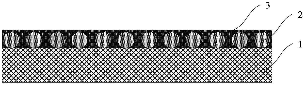
[0060] like figure 1 As shown, the present invention provides a transparent conductive film, the transparent conductive film at least includes: a target structure 1; a silver nanowire film layer, the silver nanowire film layer is located on the surface of the target structure 1, and the silver nanowire film layer The film layer is a silver nanowire film layer whose surface has been heat-treated and hydrophilically treated; a transparent conductive polymer filling layer 3, which fills the gap inside the silver nanowire film layer and covers all The silver nanowire thin film layer. The silver nanowire thin film layer after hydrophilic treatment enables the transparent conductive polymer filling layer 3 to be uniformly coated thereon.

[0061] As an example, the target structure 1 can be a target substrate or a semiconductor structure with functional devices; when the target structure 1 is a target substrate, it can be a non-flexible substrate such as quartz glass, glass, or po...

Embodiment 2

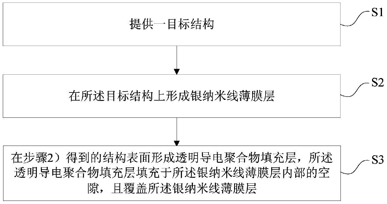
[0068] like image 3 As shown, the present invention also provides a method for making a transparent conductive film, the method for making the transparent conductive film is suitable for making the transparent conductive film described in Example 1, and the method for making the transparent conductive film includes the following steps:

[0069] 1) Provide a target structure;

[0070] 2) forming a silver nanowire film layer on the target structure;

[0071] 3) A transparent conductive polymer filling layer is formed on the surface of the structure obtained in step 2), and the transparent conductive polymer filling layer fills the gap inside the silver nanowire thin film layer and covers the silver nanowire thin film layer.

[0072] In step 1), see image 3 Step S1 in and Figure 4 , providing a target structure 1 .

[0073] As an example, the target structure 1 can be a target substrate or a semiconductor structure with functional devices; when the target structure 1 is a ...

Embodiment 3

[0102] The present invention also provides an optoelectronic device, which includes the transparent conductive film as described in the first embodiment. The optoelectronic devices include but are not limited to OLED devices and photovoltaic devices such as amorphous silicon, copper indium gallium selenide, and heterojunction (HIT) solar cells.

[0103] In summary, the present invention provides a transparent conductive film, a photoelectric device and a manufacturing method thereof. The transparent conductive film includes: a target structure; a silver nanowire film layer located on the surface of the target structure; a transparent conductive polymer filling layer , filling the void inside the silver nanowire thin film layer and covering the silver nanowire thin film layer. The transparent conductive film of the present invention has the advantages of high conductivity and high transmittance; the transparent conductive polymer filling layer can be evenly coated on it by carr...


PUM

PropertyMeasurementUnit
lengthaaaaaaaaaa
diameteraaaaaaaaaa
concentrationaaaaaaaaaa

Abstract

The invention provides a transparent conductive film, a photoelectric device and a method for preparing the transparent conductive film. The transparent conductive film includes: a target structure; asilver nanowire film layer on the surface of a target structure; a transparent conductive polymer filling layer filling voids inside the silver nanowire film layer and covering the silver nanowire film layer. The transparent conductive film has high electrical conductivity and high transmittance. The transparent conductive polymer filling layer can uniformly coats the silver nanowire film layer by subjecting the silver nanowire film layer to a hydrophilic treatment. By means of the covering of the transparent conductive polymer filling layer and a graphene film, surface roughness is reduced while high transmittance and high conductivity of the transparent conductive film are guaranteed. In addition, the transparent conductive film also has a flexible property. Bent a plurality of times, the transparent conductive film prepared on a flexible substrate has no significant change in transmittance and square resistance, and shows great potential to be applied to photoelectric devices, especially flexible photoelectric devices instead of ITO.

Description

technical field [0001] The invention belongs to the technical field of material preparation, and in particular relates to a transparent conductive film, a photoelectric device and a manufacturing method thereof. Background technique [0002] OLED (Organic Light-Emitting Diode), that is, organic electroluminescent devices, has the advantages of high luminous efficiency, fast response speed, and low driving voltage, and is one of the hot research directions in the field of optoelectronic devices. In recent years, through the continuous exploration of new materials and the continuous optimization of the device manufacturing process, OLED has made great progress, but to give full play to its advantages in the field of flat panel display, OLED device stability, cost control, flexibility, etc. Still needs further improvement. Among them, the surface work function, photoelectric characteristics, surface flatness, chemical stability and compatibility with organic layers of its tran...

Claims


Application Information

Patent Timeline
Patent Type & Authority Patents(China)
IPC IPC(8): H01L51/52H01L51/54H01L51/56H01B1/02H01B1/06H01B13/00
Inventor 方小红徐一麟王聪尤莹陈小源万吉祥
Owner SHANGHAI PYLON TECH CO LTD
Why Eureka
Try Eureka