A two-dimensional transition metal chalcogenide thin film and its preparation method
A transition metal chalcogenide, compound technology, applied in metal material coating process, liquid chemical plating, coating and other directions, to achieve the effect of easy to observe the film, conducive to energy concentration, less energy consumption
- Summary
- Abstract
- Description
- Claims
- Application Information
AI Technical Summary
Problems solved by technology
Method used
Image
Examples
preparation example Construction
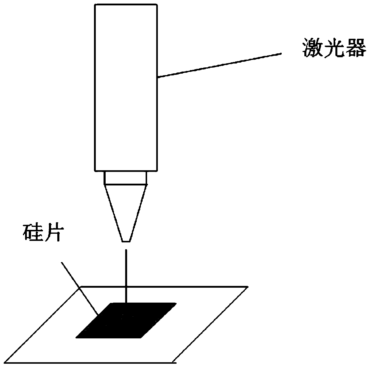
[0028] Such as figure 1 Shown, a kind of preparation method of two-dimensional transition metal chalcogenide thin film comprises:
[0029] (1) Substrate preparation: Select a silicon wafer with a size of 2 to 4 inches and an oxide layer thickness of 50 to 300 mm, and use a diamond knife to cut a single crystal silicon wafer with an oxide layer as a substrate, with a side length of 0.5 to 1.5 cm square.
[0030] (2) Precursor preparation: Weigh A and B with an electronic balance. The weight of A is 0.001g~0.1g, and the weight of B is 0.001g~0.1g. Airtight reaction for 2-4 hours, the temperature is 20-80 ° C, forming an orange-red precursor solution, A is molybdenum pentachloride or tungsten tetrachloride, B is thiourea or selenourea, C is isopropanol, ethanol or Methanol.
[0031] (3) Cleaning the substrate: use acetone to clean the cut silicon wafer, the square with a side length of 0.5-1.5cm, the purity is greater than 99.5%, ultrasonic for 5-10 minutes, and then use absol...
Embodiment 1
[0035] (1) Substrate preparation: select a silicon wafer with a size of 4 inches and an oxide layer thickness of 150 mm, and use a diamond knife to cut a single crystal silicon wafer with an oxide layer as a substrate, and the substrate is a square with a side length of 0.5 cm.
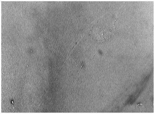
[0036] (2) Precursor preparation: such as figure 2 Weigh MoCl with electronic balance as shown 5 , with a weight of 0.02g and thiourea, with a weight of 0.1g, were put into a test tube, 5ml of isopropanol was added to the test tube, and the water bath was closed for reaction for 3 hours at a temperature of 60°C to form an orange-red precursor solution.
[0037] (3) Cleaning the substrate: Use acetone to clean the silicon wafer with a side length of 0.5 cm, sonicate for 5 minutes with a purity greater than 99.5%, then use absolute ethanol with a purity greater than 99.7%, sonicate for 5 minutes, and finally use Rinse with deionized water and sonicate for 5 minutes.
[0038] (4) Spin-coating reactant...
Embodiment 2
[0042] (1) Substrate preparation: select a silicon wafer with a size of 2 inches and an oxide layer thickness of 50 mm, use a diamond knife to cut a single crystal silicon wafer with an oxide layer as a substrate, and the substrate is a square with a side length of 1 cm.
[0043] (2) Precursor preparation: Weigh MoCl with an electronic balance 5 The weight is 0.001g, and the weight of thiourea is 0.005g. Put it into a test tube, add 1ml of isopropanol into the test tube, and react in a sealed water bath for 2 hours at a temperature of 80°C to form an orange-red precursor solution.
[0044] (3) Clean the substrate: use acetone to clean the silicon wafer with a side length of 1cm, and use acetone to make the purity greater than 99.5%, sonicate for 10 minutes, then use absolute ethanol to make the purity greater than 99.7%, sonicate for 10 minutes, and finally use Wash with deionized water and sonicate for 10 minutes.
[0045] (4) Spin-coating reactant: place the silicon wafer o...
PUM
| Property | Measurement | Unit |
|---|---|---|
| thickness | aaaaa | aaaaa |
| thickness | aaaaa | aaaaa |
| thickness | aaaaa | aaaaa |
Abstract
Description
Claims
Application Information
 - Generate Ideas
- Intellectual Property
- Life Sciences
- Materials
- Tech Scout
- Unparalleled Data Quality
- Higher Quality Content
- 60% Fewer Hallucinations
Browse by: Latest US Patents, China's latest patents, Technical Efficacy Thesaurus, Application Domain, Technology Topic, Popular Technical Reports.
© 2025 PatSnap. All rights reserved.Legal|Privacy policy|Modern Slavery Act Transparency Statement|Sitemap|About US| Contact US: help@patsnap.com


