Field effect transistor structure-based pH sensing device and manufacturing method thereof

A technology of field effect transistors and sensor devices, which is applied in the field of sensors, can solve problems such as low sensitivity, device short circuit, device process difficulty, etc., and achieve the effects of broad application prospects, fast response speed, and high sensitivity

Active Publication Date: 2017-12-22
ZHEJIANG UNIV
View PDF6 Cites 4 Cited by
  • Summary
  • Abstract
  • Description
  • Claims
  • Application Information

AI Technical Summary

Problems solved by technology

However, this sensor has the following disadvantages: 1. It is large in size and generally on the order of millimeters, and it is difficult to test the pH value of a small volume of the solution to be tested; 2. The detection speed is slow, and it is difficult to monitor the changing pH value in real time; 3. The sensitivity is not high. The sensor uses voltage as the output signal. When the pH value changes by 1, the sensor output voltage changes by tens to one hundred millivolts.
However, in this sensor structure, the distance between the floating gate and the gate oxide layer must be extremely small (on the order of nanometers), otherwise the floating gate will lose its ability to electrically control the device.
This has caused great difficulty in the device process
On the other hand, since the solution to be tested is generally conductive, when the solution to be tested is filled between the floating gate and the gate oxide layer, it is easy to cause a short circuit of the device

Method used


Image

  • Field effect transistor structure-based pH sensing device and manufacturing method thereof
  • Field effect transistor structure-based pH sensing device and manufacturing method thereof
  • Field effect transistor structure-based pH sensing device and manufacturing method thereof

Examples


Embodiment 1

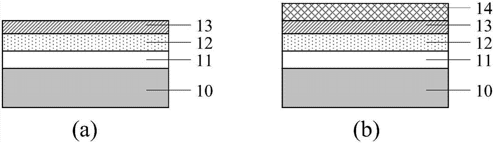
[0057] Embodiment 1: In this embodiment, a silicon substrate on an insulating layer is used, and the preparation method and the working principle and electrical output characteristics of the pH sensor device are as follows:

[0058] (1) if figure 1 As shown in (a), the front gate oxide layer 13 is deposited on the silicon layer of the silicon substrate on the insulating layer, the deposition method is thermal oxidation, atomic layer deposition or sputtering, and the thickness is 1 nanometer to 10 nanometers;

[0059] (2) if figure 1 As shown in (b), the gate layer 14 is deposited on the front gate oxide layer 13, the deposition method is evaporation or sputtering, and the thickness is tens to hundreds of nanometers;

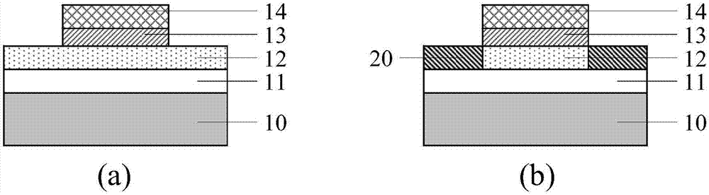
[0060] (3) if figure 2 As shown in (a), the gate layer 14 and the front gate oxide layer 13 are removed by an etching process until the silicon layer surface of the silicon substrate on the insulating layer to form a gate structure of a field effect transistor...


PUM

PropertyMeasurementUnit
thicknessaaaaaaaaaa

Abstract

The present invention discloses a field effect transistor structure-based pH sensing device and a manufacturing method thereof. The manufacturing method is as follows: firstly, a front gate oxide layer and a gate layer are deposited on the surface of a semiconductor layer of a semiconductor substrate on an insulating layer, a gate electrode structure is formed by etching of the front gate oxide layer and the gate layer; secondly, a source-drain structure is formed by doping of the semiconductor layer of the semiconductor substrate on the insulating layer on both sides of the gate electrode structure, and the gate electrode structure and the source-drain structure together form a field-effect transistor structure; and further, photolithography is performed on the back surface of a silicon substrate on the insulating layer, a supporting substrate and a buried oxide layer are etched until the lower surface of the semiconductor layer, and a back gate oxide layer is deposited on the lower surface of the etched semiconductor layer to complete the preparation of the pH sensing device. The method utilizes the contact between a solution to be tested and a back gate of the field-effect transistor to form a double-electric-layer structure on the surface of the back gate, by changing of the Zeta potential of the double-electric-layer on the surface of the back gate in different pH solutions, the threshold voltage of the field-effect transistor can be changed, the change of the resistance of the sensing device under a fixed bias voltage can be further led, the pH value of the solution can be tested.

Description

technical field [0001] The invention belongs to the field of sensors, and relates to a structure of a high-performance pH value sensor and a manufacturing method thereof. Background technique [0002] The pH value is an important indicator for evaluating the chemical state of water bodies, and it has high reference value in reflecting the concentration of pollutants in water bodies, microbial activities, and various physical signs of the human body. Therefore, pH value detection plays an important role in many fields such as chemical industry, aquatic products, water quality monitoring, environmental governance, and medical care. In the pH value detection equipment, the most critical part is the pH value sensor. The pH value sensor generally has the following requirements: 1. High detection accuracy, sensitive to pH value changes, and able to accurately obtain the pH value of the solution to be tested; 2. Detection The speed is fast, and the pH value of the water body can b...

Claims


Application Information

Patent Timeline
Patent Type & Authority Applications(China)
IPC IPC(8): G01N27/414
CPCG01N27/4146
Inventor 张睿赵毅
Owner ZHEJIANG UNIV
Why Eureka
Try Eureka