Process method of trench type dual-layer-gate MOS dielectric layer

A process method and dielectric layer technology, applied in electrical components, semiconductor/solid-state device manufacturing, semiconductor devices, etc., can solve the problems of easy breakdown of gate polysilicon and low yield, improve gate/source leakage, optimize film texture, the effect of increasing thickness

Inactive Publication Date: 2017-12-19
SHANGHAI HUAHONG GRACE SEMICON MFG CORP
View PDF8 Cites 1 Cited by
  • Summary
  • Abstract
  • Description
  • Claims
  • Application Information

AI Technical Summary

Problems solved by technology

But its disadvantages are also obvious: the ratio of film formation on polysilicon to silicon is 1:3, and the gate oxide deposition thickness is 1:3. The target calculation, the dielectric layer thickness reaches Leakage close to SPEC
[0003] In addition, there are weak spots at the bottom of the gate polysilicon that are easy to break down (such as figure 1 Arrow pointing), the distance from the source polysilicon There is a risk of low yield

Method used


Image

  • Process method of trench type dual-layer-gate MOS dielectric layer
  • Process method of trench type dual-layer-gate MOS dielectric layer
  • Process method of trench type dual-layer-gate MOS dielectric layer

Examples


Embodiment Construction

[0021] The process method of the trench-type double-layer gate MOS dielectric layer according to the present invention comprises:

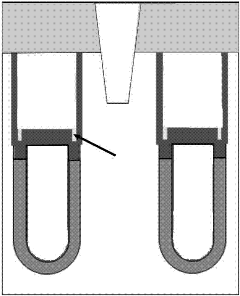
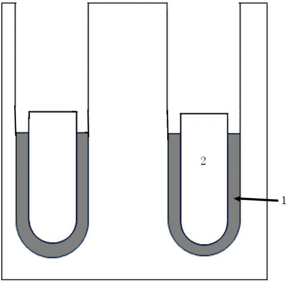
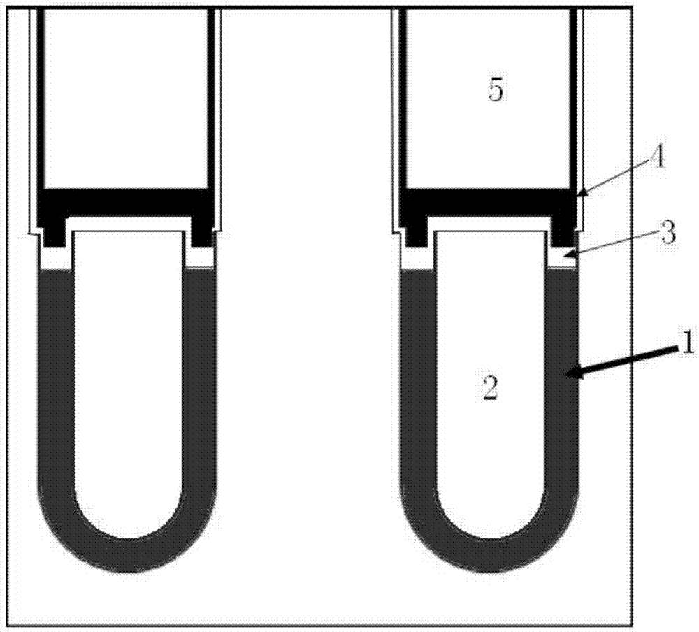
[0022] Step 1, such as figure 2 As shown, a groove is formed by etching on the silicon substrate, and a dielectric layer 1 is grown inside the groove. The dielectric layer includes a thermal oxide layer and a composite liner film layer of oxide film / nitride film / oxide film; or thermal oxidation Add a nitride film layer; and fill the trench with polysilicon 2 for the first time, etch back the polysilicon and the dielectric layer, leaving the upper half of the trench free, and the remaining polysilicon at the bottom as the source.

[0023] The second step is to perform thermal oxidation to form a thermal oxide layer 3 and deposit a high-density plasma oxide film 4; then perform a second polysilicon deposition 5 to fill the trench, and then perform polysilicon etching back, that is, etching back to the trench The polysilicon in the groove is flush ...


PUM


Abstract

The invention discloses a method for optimizing a trench type dual-layer-gate MOS dielectric layer structure. The method comprises the steps of 1, etching a silicon substrate to form a trench, enabling a dielectric layer to be grown in the trench, performing polysilicon filling in the trench for the first time, performing back etching on the polysilicon and the dielectric layer, and keeping the upper half part of the trench blank; 2, performing thermal oxidization to form a thermal oxide layer and performing deposition of a high-density plasma oxidization film; performing polysilicon deposition for the second time and full filling of the trench, and next, performing back etching of polysilicon; and 3, performing back etching of the thermal oxide layer; performing base and source injection; forming an interlayer film; etching contact holes and depositing metal; and depositing a passivation layer. By virtue of the method, the film structure of the dielectric layer is optimized, namely, the thickness of the dielectric layer is increased by the combination of thermal oxidization and the high-density plasma oxidization film, so that the distance between the polysilicon for forming the gate and the polysilicon for forming the source is enlarged, thereby relieving gate/source electric leakage, and solving the problem of the weak region at the bottom of the polysilicon for forming the gate.

Description

technical field [0001] The invention relates to the field of semiconductors, in particular to a process method for a trench-type double-layer gate MOS dielectric layer. Background technique [0002] Ordinary trench double-layer gate MOS devices such as figure 1 As shown, the trench is located in the silicon substrate, and the inner wall of the trench is attached with an insulating dielectric layer. The trench is divided into upper and lower parts of polysilicon, the lower layer is the source polysilicon of the MOS device, and the upper layer is the gate (polysilicon) of the MOS device. . The upper and lower layers of polysilicon are separated by a gate oxide layer and a dielectric layer. The current method of forming a dielectric layer between two layers of polysilicon uses the difference in the film thickness of the thermal oxide layer on the silicon and the source polysilicon, and simultaneously generates GOX (gate oxide) and IPO (dielectric layer), and the process is si...

Claims


Application Information

Patent Timeline
Patent Type & Authority Applications(China)
IPC IPC(8): H01L21/28
CPCH01L21/28035
Inventor 陈晨
Owner SHANGHAI HUAHONG GRACE SEMICON MFG CORP
Why Eureka
Try Eureka