
Transparent electrode based on ultra-thin metallic film and preparation method and application thereof

A technology of transparent electrodes and ultra-thin metals, applied in the field of electrodes, can solve problems such as affecting compatibility, increasing costs, and poor mechanical flexibility of ITO, achieving the effects of improving optical performance, increasing aperture ratio, and increasing degrees of freedom

Active Publication Date: 2017-11-24
NINGBO INST OF MATERIALS TECH & ENG CHINESE ACADEMY OF SCI
View PDF7 Cites 18 Cited by
  • Summary
  • Abstract
  • Description
  • Claims
  • Application Information

AI Technical Summary

Problems solved by technology

However, ITO products have the following problems: (1) the mineable amount of indium element is limited, and the cost is increasing; (2) the mechanical flexibility of ITO is poor, which is difficult to meet the application requirements of new flexible optoelectronic devices; (3) high temperature (several Hundred degrees Celsius) post-deposition treatment to mainly improve their electrical properties, this high temperature process will affect its compatibility with some active materials or organic composite materials
However, the multi-layer structure will inevitably increase the cost and process complexity

Method used


Image

  • Transparent electrode based on ultra-thin metallic film and preparation method and application thereof
  • Transparent electrode based on ultra-thin metallic film and preparation method and application thereof
  • Transparent electrode based on ultra-thin metallic film and preparation method and application thereof

Examples


Embodiment 1

[0040] (1) Ultra-clear glass with a thickness of 1mm was used as a transparent substrate, and the glass was ultrasonically cleaned with acetone, ethanol, and deionized water, and dried with N 2 Blow dry, and then treat the glass surface with ultraviolet ozone for 20 minutes, then put it into the magnetron sputtering chamber immediately, and start vacuuming.

[0041] (2) Wait until the vacuum degree of the magnetron sputtering chamber reaches 5×10 -4 Below Pa, feed 40sccm high-purity argon as the deposition gas. A DC sputtering metal Ag target was used, the DC sputtering power was 20W, and the sputtering time was controlled to obtain a 9nm thick Ag film. After the film deposition was completed, the sample was taken out to obtain a glass / Ag (9nm) sample. During the preparation process, the substrate temperature was room temperature, and the substrate was kept rotating to ensure the uniformity of the film.

[0042] (3) Deposit 30nm TiO on the Ag layer plated in step (2) 2 film...

Embodiment 2

[0046] (1) Ultra-clear glass with a thickness of 1mm was used as a transparent substrate, and the glass was ultrasonically cleaned with acetone, ethanol, and deionized water, and dried with N 2 Blow dry, and then treat the glass surface with ultraviolet ozone for 20 minutes.

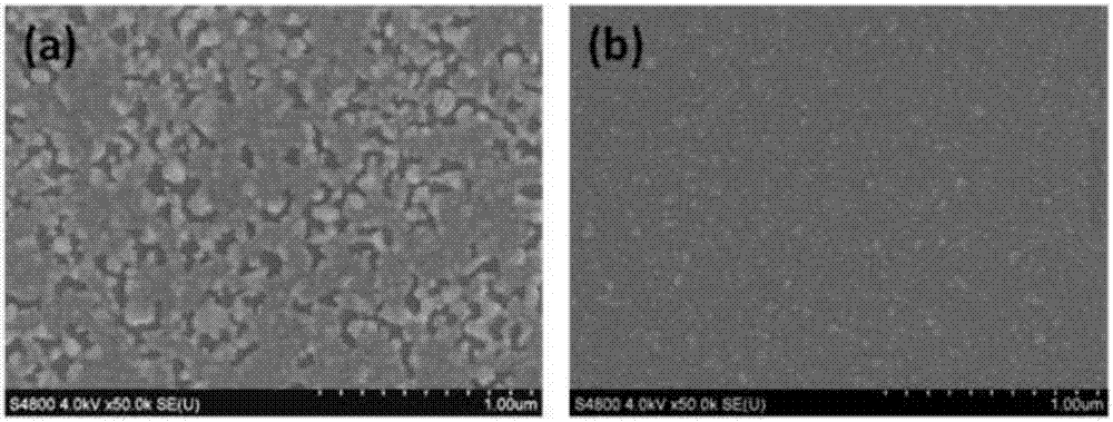
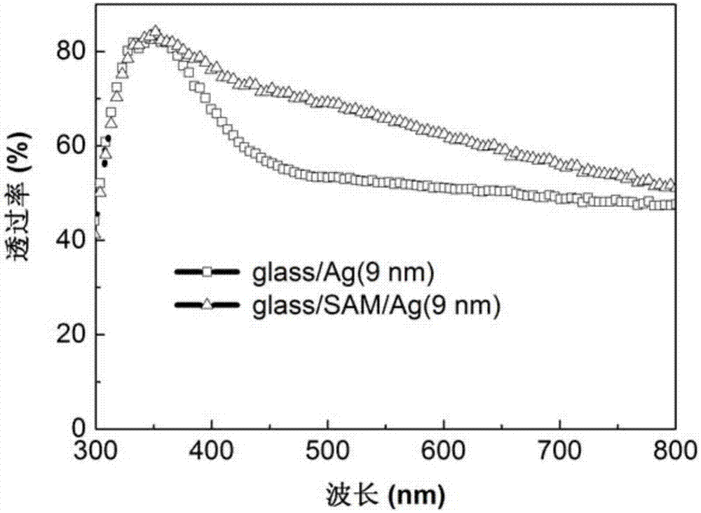
[0047] (2) Prepare a self-assembly solution, the components of which are isopropanol, deionized water and 3-aminopropyltrimethoxysilane, with a volume ratio of 18:1:1. Immerse the glass cleaned in step (1) in the self-assembly solution for 2 hours. Rinse with isopropanol and rinse with N 2 Dry it, then put it into the magnetron sputtering chamber immediately, and start vacuuming.

[0048] (3) Wait until the vacuum degree of the magnetron sputtering chamber reaches 5×10 -4 Below Pa, feed 40sccm high-purity argon as the deposition gas. A metal Ag target was sputtered by direct current, the direct current sputtering power was 20W, and the sputtering time was controlled to obtain a 9nm thick Ag film. Af...

Embodiment 3

[0056] (1) Ultra-clear glass with a thickness of 1mm was used as a transparent substrate, and the glass was ultrasonically cleaned with acetone, ethanol, and deionized water, and dried with N 2 Dry it, then put it into the magnetron sputtering chamber immediately, and start vacuuming.

[0057] (2) Wait until the vacuum degree of the magnetron sputtering chamber reaches 5×10 -4 Below Pa, feed 40sccm high-purity argon as the deposition gas. A DC sputtering metal Ag target was used, the DC sputtering power was 20W, and the sputtering time was controlled to obtain a 6nm thick Ag film. After the film deposition was completed, the sample was taken out to obtain a glass / Ag (6nm) sample. During the preparation process, the substrate temperature was room temperature, and the substrate was kept rotating to ensure the uniformity of the film. The above Ag film deposition rates have been determined by ellipsometer measurements.

[0058] (3) Depositing a 40nm AZO thin film on the Ag laye...


PUM

PropertyMeasurementUnit
Thicknessaaaaaaaaaa
Thicknessaaaaaaaaaa
Thicknessaaaaaaaaaa

Abstract

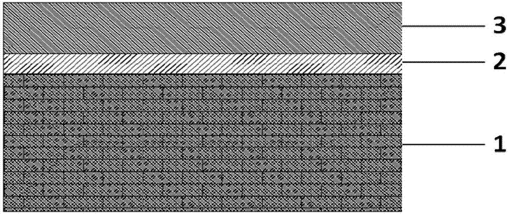
The invention discloses a transparent electrode based on an ultra-thin metallic film. The transparent electrode orderly comprises a transparent substrate, a metal layer and a metal oxide layer from bottom to top, wherein the thickness of the metal layer is 3 to 12nm. The substrate is modified by a monomolecular self-assembled layer; an ultra-thin metal layer is directly deposited on the substrate, and the continuity and conductivity of the ultra-thin metallic film are improved through the function of the monomolecular self-assembled layer; or through the co-deposition of metals, the continuous growth of the ultra-thin metallic film is realized directly on the substrate; and a metal oxide layer is deposited on the substrate as an antireflection layer, then a double-layer film system structure is obtained, and through the design and optimization of the double-layer film system structure, the maximization of transmittance is realized. The invention further discloses a preparation method of the transparent electrode based on the ultra-thin metallic film and an application thereof in photoelectric devices, wherein the transparent electrode can have good conductivity and high transmittance at the same time.

Description

technical field [0001] The invention belongs to the technical field of electrodes, and in particular relates to a transparent electrode based on an ultra-thin metal film and a preparation method and application thereof. Background technique [0002] Transparent conductive films, because of their high transmittance in visible light and low resistivity, are widely used in various optoelectronic devices, including solar cells, image sensors, liquid crystal displays, organic electroluminescent (OLED) and touch screen panels. From an application point of view, in addition to large optical transparency in the required wavelength range and appropriate conductivity, transparent electrodes should also have other advantages such as ease of processing (e.g., possibility of large-scale deposition), and the ability to form the same device ( For example, compatibility with other materials of the active layer), stability with respect to temperature, mechanical and chemical stress, and the ...

Claims


Application Information

Patent Timeline
IPC IPC(8): H01L31/0224H01L33/42H01L31/18
CPCH01L31/022425H01L31/022466H01L31/1888H01L33/42Y02P70/50
Inventor 宋伟杰黄金华李佳杨晔许君君鲁越晖朱超挺
Owner NINGBO INST OF MATERIALS TECH & ENG CHINESE ACADEMY OF SCI
Learn More