Display substrate manufacturing method

A manufacturing method and display substrate technology, applied in the direction of instruments, semiconductor devices, electrical components, etc., can solve the problems affecting the image display stability of the display device, pixel brightness unevenness, etc., to ensure stability, good photosensitivity, and exposure energy small effect

Active Publication Date: 2017-11-24
BOE TECH GRP CO LTD
View PDF3 Cites 0 Cited by
  • Summary
  • Abstract
  • Description
  • Claims
  • Application Information

AI Technical Summary

Problems solved by technology

[0006] In order to solve the problem in the related art that the pixel brightness on the display device may be uneven when manufacturing the display substrate and affect the image display stability of the display device, an embodiment of the present invention provides a method for manufacturing a display substrate

Method used


Image

  • Display substrate manufacturing method
  • Display substrate manufacturing method
  • Display substrate manufacturing method

Examples


Embodiment Construction

[0040] In order to make the object, technical solution and advantages of the present invention clearer, the implementation manner of the present invention will be further described in detail below in conjunction with the accompanying drawings.

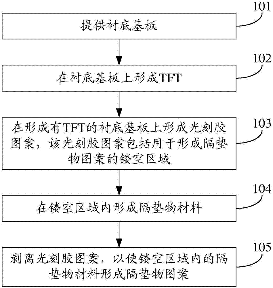
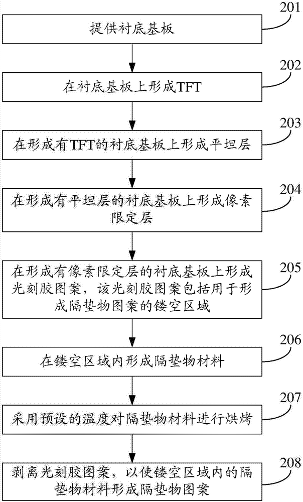
[0041] At present, when the display substrate is manufactured, the pixel brightness on the display device may be uneven, which affects the image display stability of the display device. In order to solve this problem, an embodiment of the present invention provides a method for manufacturing a display substrate, such as figure 1 As shown, the method may include:

[0042] Step 101, providing a base substrate.

[0043] Step 102, forming a TFT on the base substrate.

[0044] Step 103 , forming a photoresist pattern on the base substrate on which the TFT is formed, the photoresist pattern including a hollow area for forming a spacer pattern.

[0045] Step 104 , forming a spacer material in the hollow area.

[0046] Step 105 , stripping ...


PUM

PropertyMeasurementUnit
thicknessaaaaaaaaaa

Abstract

The invention discloses a display substrate manufacturing method and belongs to the technical field of display. The method comprises the following steps: providing a substrate; forming a thin film transistor (TFT) on the substrate; forming a photoresist pattern on the substrate having the TFT formed thereon, wherein the photoresist pattern comprises a hollow area for forming a spacer pattern; forming spacer material in the hollow area; and stripping the photoresist pattern to enable the spacer material in the hollow area to form the spacer pattern. The display substrate manufacturing method solves the problem that image display stability of a display device is influenced due to possible pixel brightness nonuniformity of the display device when the display substrate is prepared in the prior art. The method is used for manufacture of the display substrate.

Description

technical field [0001] The invention relates to the field of display technology, in particular to a method for manufacturing a display substrate. Background technique [0002] An organic light-emitting diode (English: Organic Light-Emitting Diode; abbreviation: OLED) display device is a display device with an autonomous light emitting function. The OLED display device includes a plurality of pixels arranged in a matrix, and the OLED display device can be divided into an active matrix organic light emitting diode (English: ActiveMatrix / Organic Light Emitting Diode; abbreviation: AMOLED) display device and an OLED display device according to the driving method of its pixels. Source matrix organic light-emitting diode (English: Passive matrix Organic Light-Emitting Diode; abbreviation: PMOLED) display device, among which, AMOLED display device is characterized by its thin thickness, light weight, active light emission, fast response speed, wide viewing angle, rich colors and hi...

Claims


Application Information

Patent Timeline
Patent Type & Authority Applications(China)
IPC IPC(8): H01L27/32
CPCH10K59/124H10K59/1201G02F1/13394H10K59/122H10K50/8428H01L27/1214H01L25/50H01L25/075G02F1/13396G02F1/13398H10K59/123H10K59/1213
Inventor 张锋吕志军刘文渠董立文张世政党宁刘志勇
Owner BOE TECH GRP CO LTD
Why Eureka
Try Eureka