Chip fixed resistor and manufacturing method therefor

A technology of fixed resistance and manufacturing method, which is applied in the direction of resistance terminals/electrodes, resistors with lead-out terminals, manufacturing package/shell resistors, etc., which can solve the problems of low repeatability, poor product consistency, and low product accuracy, etc. Achieve the effect of good repeatability, good high frequency characteristics and high product accuracy

Inactive Publication Date: 2017-11-17
CHINA ZHENHUA GRP YUNKE ELECTRONICS
View PDF10 Cites 4 Cited by
  • Summary
  • Abstract
  • Description
  • Claims
  • Application Information

AI Technical Summary

Problems solved by technology

[0003] At present, most of the high-precision alloy foil fixed resistors on the market are plug-in alloy foil fixed resistors. Plug-in alloy foil fixed resistors include the lead segment of the resistor. The volume is large and the thickness is very high, which does not meet the needs of the miniaturization of components in the market today, and it is a waste of cost. The product consistency is poor, the repeatability is low, the product accuracy is low, the reliability is low, and it is not convenient to weld

Method used


Image

  • Chip fixed resistor and manufacturing method therefor
  • Chip fixed resistor and manufacturing method therefor
  • Chip fixed resistor and manufacturing method therefor

Examples


Embodiment 1

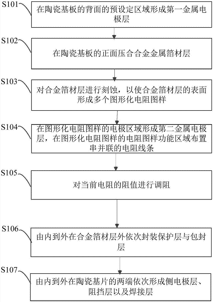
[0047] see figure 1 , this embodiment provides a method for manufacturing a chip fixed resistor, the method for manufacturing a chip fixed resistor includes:

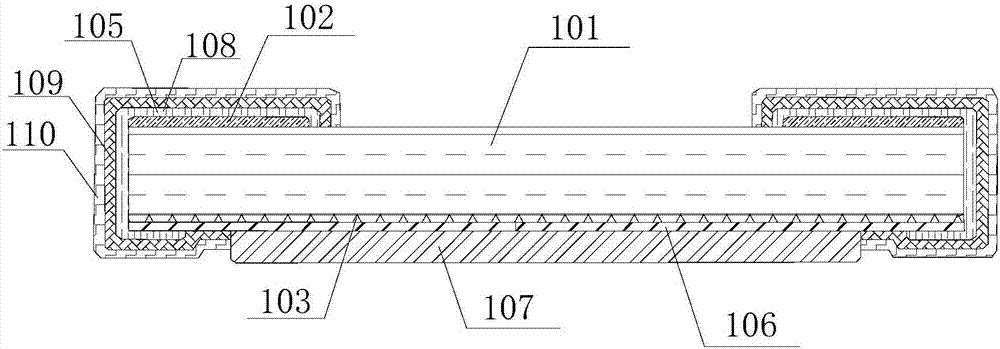
[0048] Step S101 : forming a first metal electrode layer 102 on a predetermined area on the back of a ceramic substrate 101 .

[0049]The ceramic substrate 101 has excellent electrical insulation performance, high thermal conductivity and high adhesion strength, and can etch various patterns like a PCB board, and has a large current-carrying capacity. Therefore, the ceramic substrate 101 can be used as a basic material for high-power power electronic circuit structure technology and interconnection technology. In this embodiment, the first metal electrode layer 102 may be formed on a predetermined area on the back of the ceramic substrate 101 by, but not limited to, sputtering, evaporation or screen printing.

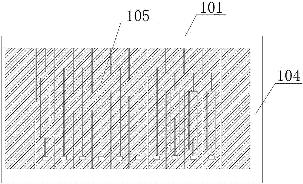
[0050] Step S102 : pressing the alloy foil layer 103 on the front surface of the ceramic substrate 101 .

...


PUM

PropertyMeasurementUnit
thicknessaaaaaaaaaa

Abstract

The invention provides a method for manufacturing a chip-type fixed resistor and the chip-type fixed resistor, and relates to the field of electronic components. Firstly, the first metal electrode layer is formed in a predetermined area on the back of a ceramic substrate; then the alloy foil layer is laminated on the front of the ceramic substrate; and then the alloy foil layer is etched to make the surface of the alloy foil layer Form a patterned resistance pattern; then form a second metal electrode layer in the electrode area of ​​the patterned resistance pattern, and arrange series and parallel resistance lines in the resistance pattern functional area of ​​the patterned resistance pattern; finally, from the inside to the outside outside the alloy foil layer Encapsulating the protective layer and the encapsulation layer in sequence; forming a side electrode layer, a barrier layer and a welding layer at both ends of the ceramic substrate from the inside to the outside. The thickness of the chip fixed resistor is low, which meets the needs of device miniaturization in the current market. It has good repeatability, high product precision, low temperature drift, low noise, good high-frequency characteristics, no inductance and no tolerance, and is convenient for welding.

Description

technical field [0001] The invention relates to the field of electronic components, in particular, to a method for manufacturing a chip-type fixed resistor and the chip-type fixed resistor. Background technique [0002] Resistors are generally directly referred to as resistances in daily life. It is a current-limiting element. After the resistor is connected to the circuit, the resistance value of the resistor is fixed. Generally, there are two pins, which can limit the current through the branch it is connected to. A resistor whose resistance value cannot be changed is called a fixed resistor. Those with variable resistance are called potentiometers or variable resistors. An ideal resistor is linear, that is, the instantaneous current through the resistor is proportional to the instantaneous applied voltage. A variable resistor for voltage division, with one or two movable metal contacts tightly pressed against the exposed resistor body. The position of the contacts det...

Claims


Application Information

Patent Timeline
Patent Type & Authority Applications(China)
IPC IPC(8): H01C17/02H01C17/28H01C1/02H01C1/14
CPCH01C17/02H01C1/02H01C1/14H01C17/28
Inventor 史书刚韩玉成陈天磊朱威禹廖东刘艳
Owner CHINA ZHENHUA GRP YUNKE ELECTRONICS
Why Eureka
Try Eureka