
Infrared detector and preparation method thereof

An infrared detector and structure layer technology, applied in the field of image sensors, can solve the problems of limited compensation capability, poor uniformity, and rising cost, and achieve the effects of improving device integration, improving detection sensitivity, and saving proportions

Active Publication Date: 2017-11-07
SHANGHAI INTEGRATED CIRCUIT RES & DEV CENT
View PDF5 Cites 0 Cited by
  • Summary
  • Abstract
  • Description
  • Claims
  • Application Information

AI Technical Summary

Problems solved by technology

[0003] However, in the structure of the traditional infrared image sensor, since the blind element array and the pixel array are not in the same area, the environment of the blind element array and the pixel array is not the same, which will lead to the difference between the blind element array and the pixel array. The difference in thermal noise ultimately affects the detection sensitivity of infrared image sensors
[0004] In addition, the sensitive layer of the traditional uncooled infrared detector is a planar structure, and the sensitive layer is sandwiched between the upper and lower electrodes.
In the design of traditional resistors, the resistance value is affected by many factors such as photolithography and etching size, film thickness, etc., resulting in poor uniformity; after the uniformity of sensitive resistors in the array becomes poor, it is necessary to increase the resistance value through ASIC circuit design. Compensation resistors are used to compensate, but the compensation capability of this technology is limited, and it will increase the complexity and cost of the circuit, resulting in a decrease in the overall performance of the product and an increase in cost
In addition, due to the high resistivity of some sensitive materials, reducing the bias voltage must reduce the design value of the sensitive resistance. At this time, it is very difficult for the traditional planar structure

Method used


Image

  • Infrared detector and preparation method thereof
  • Infrared detector and preparation method thereof
  • Infrared detector and preparation method thereof

Examples


Embodiment Construction

[0044] In order to make the content of the present invention clearer and easier to understand, the content of the present invention will be further described below in conjunction with the accompanying drawings. Of course, the present invention is not limited to this specific embodiment, and general replacements known to those skilled in the art are also covered within the protection scope of the present invention.

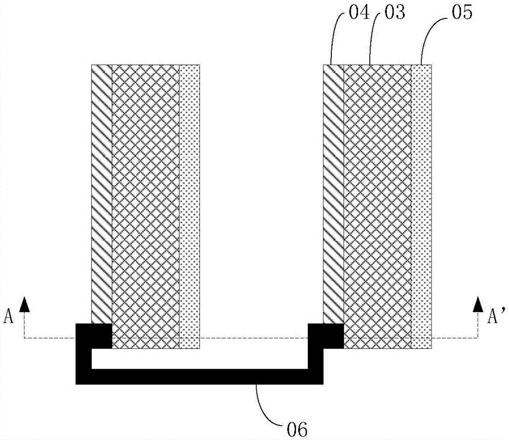
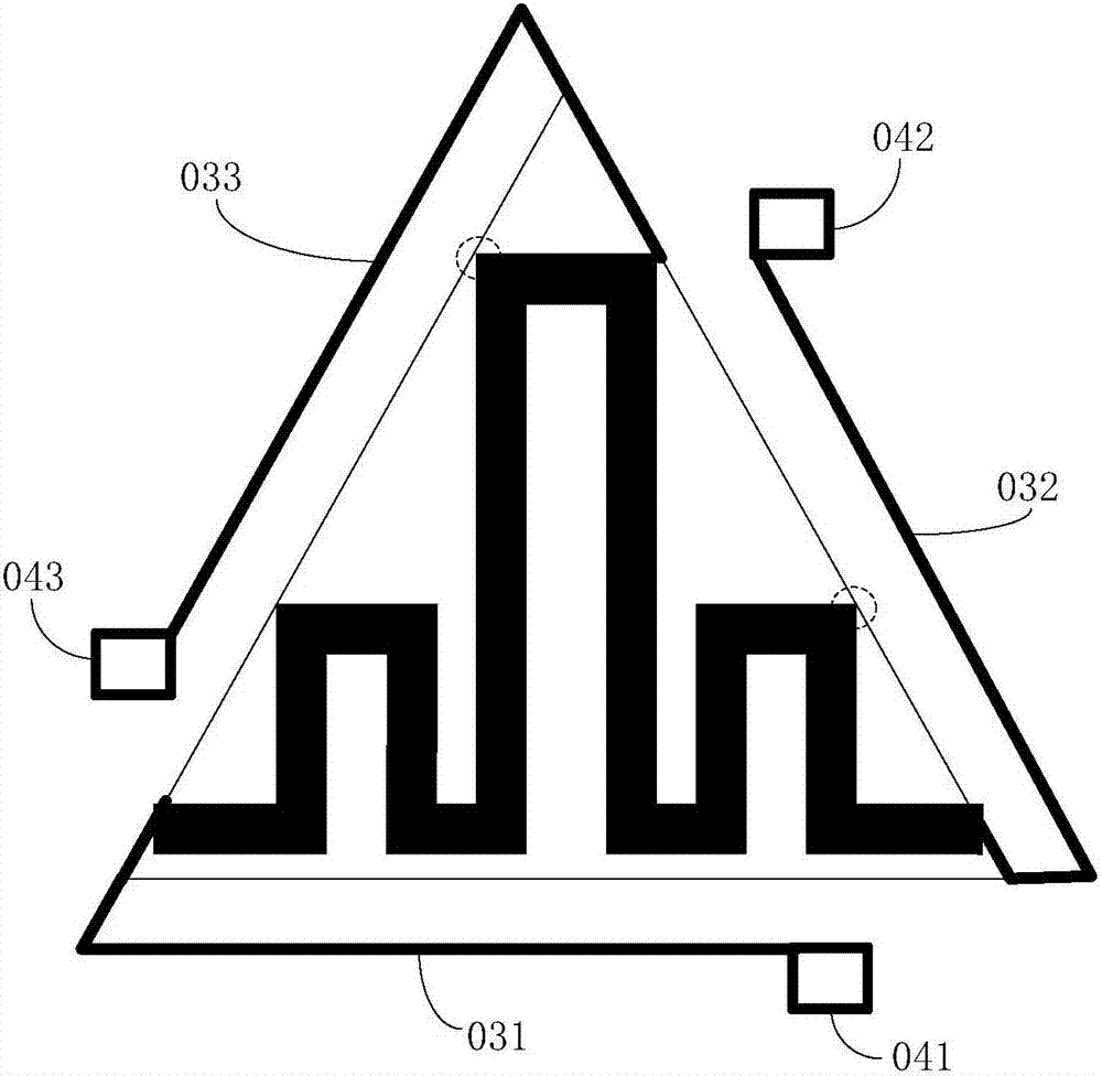
[0045]An infrared detector of the present invention has an effective pixel array, and each effective pixel in the effective pixel array includes a detection structure layer and a blind element structure layer; the detection structure layer and the blind element structure layer are respectively located in a non- doping the two sidewall surfaces of the fin structure.

[0046] In the structural design of the image sensor of the present invention, the design distribution of the existing effective pixel array and the blind pixel array is changed, and the blind pixel arr...


PUM


Abstract

The invention provides an infrared detector and a preparation method thereof. A detection structure layer and a blind pixel structure layer are arranged in each effective pixel in an effective pixel array; and the detection structure layer and the blind pixel structure layer are respectively located in both sidewall surfaces of a non-doped fin structure. According to the invention, the detection structure layer and the blind pixel structure layer are integrated in the same effective pixel, the proportion of pixels is saved and the device integration is improved, the flexible adjustment of the resistance of the infrared detector can also be realized without being affected by the lithography and thin film thickness, and the detection sensitivity is further improved.

Description

technical field [0001] The invention relates to the technical field of image sensors, in particular to an infrared detector and a preparation method thereof. Background technique [0002] In the traditional infrared image sensor chip design, the blind element array and the effective pixel array are not in the same area at all. Usually, one row (or several rows) or one column (or several columns) are arranged outside the effective pixel array to design blind elements. array, and share the blind element structure through the control signal in the same column, and eliminate the influence of thermal noise on the sensitivity through the difference in infrared heat sensitivity between the blind element array and the pixel array. [0003] However, in the structure of the traditional infrared image sensor, since the blind element array and the pixel array are not in the same area, the environment of the blind element array and the pixel array is not the same, which will lead to the ...

Claims


Application Information

Patent Timeline
IPC IPC(8): H01L27/146
CPCH01L27/14605H01L27/14607H01L27/14687
Inventor 康晓旭
Owner SHANGHAI INTEGRATED CIRCUIT RES & DEV CENT
Learn More