
Variable light distribution device based on silicon-based nitride and preparation method thereof

A nitride and light distribution technology, applied in optical components, TV system components, semiconductor/solid-state device components, etc., can solve the problems of limiting device integration and miniaturization, high production costs, and cumbersome processes, and achieve The preparation method is simple and easy, the processing technology is stable, and the effect of good repeatability

Active Publication Date: 2017-09-22
NANJING UNIV OF POSTS & TELECOMM
View PDF10 Cites 0 Cited by
  • Summary
  • Abstract
  • Description
  • Claims
  • Application Information

AI Technical Summary

Problems solved by technology

[0004] However, in the prior art, the Si-based MEMS microelectromechanical system and the light source are still integrated into a complete device through bonding technology. This bonding technology limits the integration and miniaturization of the device, and the structure is complex and the process is cumbersome. , high production cost, poor performance

Method used


Image

  • Variable light distribution device based on silicon-based nitride and preparation method thereof
  • Variable light distribution device based on silicon-based nitride and preparation method thereof
  • Variable light distribution device based on silicon-based nitride and preparation method thereof

Examples


Embodiment Construction

[0034] The present invention will be described in further detail below in conjunction with the accompanying drawings.

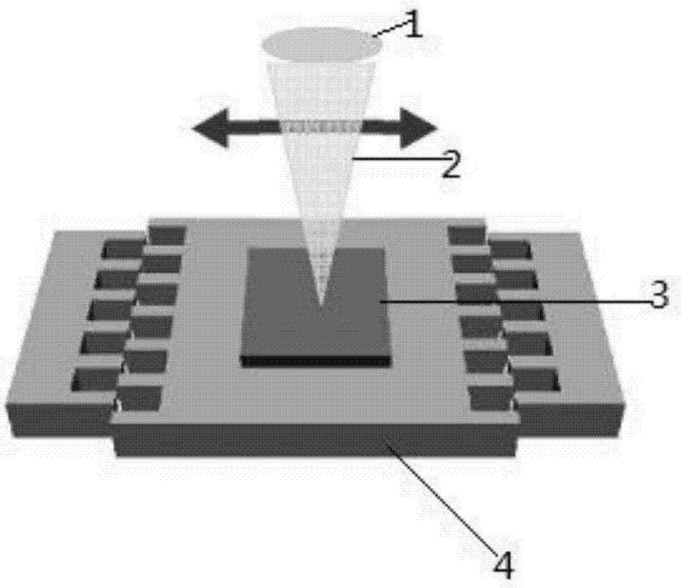
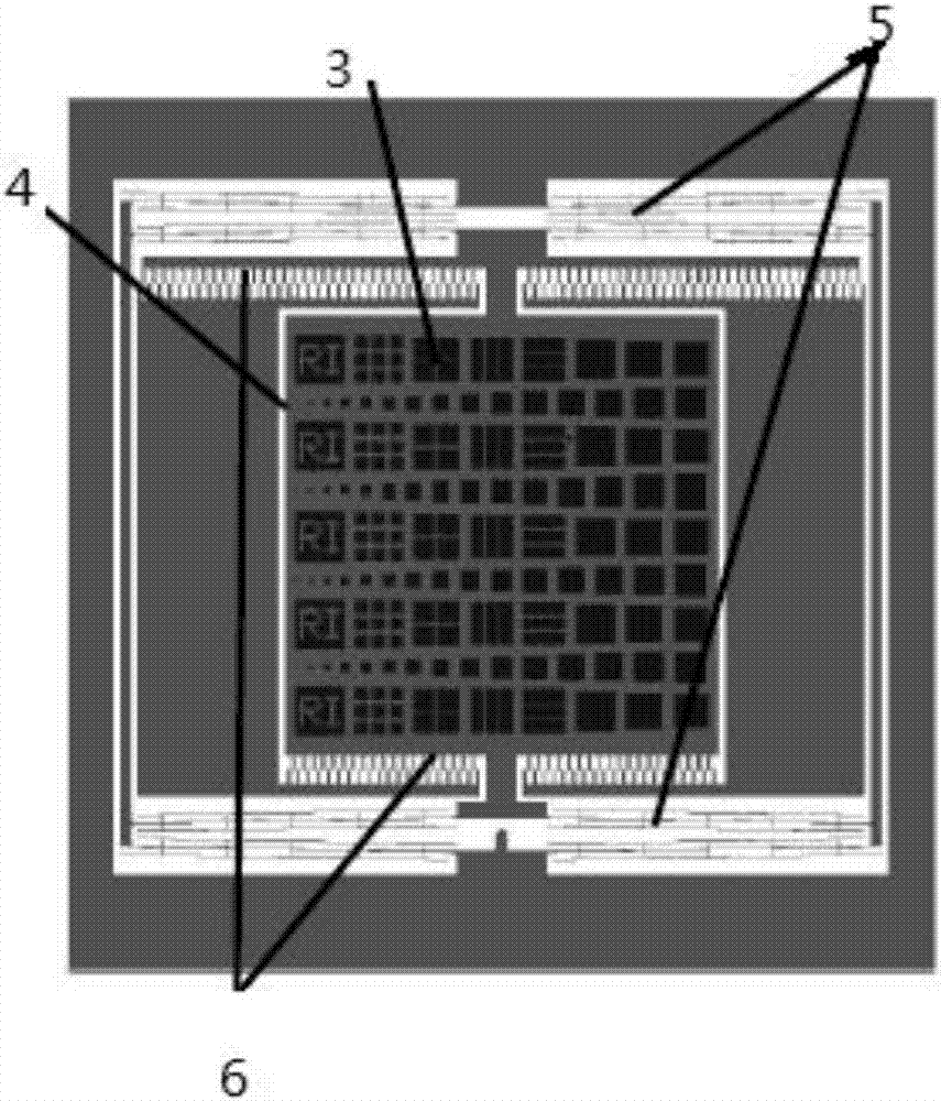
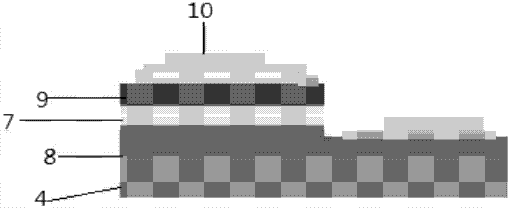
[0035] figure 1 It is a schematic diagram of the overall structure of an embodiment of the silicon-based nitride-based variable light distributor of the present invention. Such as figure 1 As shown, the variable light distributor of this embodiment includes: lens 1, GaN-based LED light source 3, Si substrate 4, electrostatic MEMS micro-actuator 60, comb driver 61, quantum well GaN 7, N-GaN 8, P-GaN 9, EL electrode 10; the GaN-based LED light source is grown on the Si substrate 4; the lens 1 is completely adhered to the GaN-based LED light source 3; the electrostatic MEMS micro-actuator 60 includes A comb driver 61 composed of a fixed-toothed comb and a movable-toothed comb; the fixed-toothed comb is connected to the Si substrate 4, and the movable-toothed comb is fixed under the GaN-based LED light source 3; by applying a voltage, the GaN-based The LED lig...


PUM

PropertyMeasurementUnit
sizeaaaaaaaaaa

Abstract

The invention discloses a variable light distribution device based on silicon-based nitride and a preparation method thereof. The variable light distribution device comprises a lens, a quantum well GaN, P-GaN, N-GaN, an EL electrode, a GaN-based LED light source, an electrostatic MEMS (Micro-Electro-Mechanical System) micro performer and a Si substrate. The GaN-based LED light source is grown on the Si substrate. The lens is completely adhered right above the GaN-based LED light source. The electrostatic MEMS micro performer comprises a comb-shaped structure composed of fixed combs and movable combs. The fixed combs are connected with the Si substrate. The movable combs and the GaN-based LED light source are fixed together. The LED light source is arranged right above the movable combs. Through application of a voltage, the GaN-based LED light source carries out lateral movement on the Si substrate plane under the drive of a comb-shaped driver. When the GaN-based LED light source moves to an optical axis direction of the lens in parallel, collimated beams passing through the GaN-based LED light source are deflected according to an angle forming certain proportion with the Si substrate plane. The device can be applied to fields such as directional illumination, free space optical communication and a robot optical sensor.

Description

technical field [0001] The invention relates to a variable light distribution device, in particular to a silicon-based nitride-based variable light distribution device and a preparation method thereof. Background technique [0002] Micro-Electro-Mechanical Systems (MEMS, Micro-Electro-Mechanical System), also known as micro-electro-mechanical systems, micro-systems, micro-machines, etc., are developed on the basis of microelectronics technology (semiconductor manufacturing technology), integrating lithography, corrosion , thin film, LIGA, silicon micromachining, non-silicon micromachining and precision machining technologies to produce high-tech electromechanical devices. MEMS technology is a high-tech cutting-edge technology that integrates various micro-processing technologies and applies modern information technology to design, process, manufacture, measure and control micro and nano materials. Various devices based on MEMS technology have been widely used in high-precis...

Claims


Application Information

Patent Timeline
Patent Type & Authority Applications(China)
IPC IPC(8): B81B7/02B81C1/00
Inventor 胡芳仁张雪花
Owner NANJING UNIV OF POSTS & TELECOMM
Learn More