
InGaN photon monolithic integration based multi-dimensional space visible light communication system

A technology of visible light communication and monolithic integration, which is applied in the field of visible light communication, can solve the problems of large spectrum and spectrum resources and inability to reverse communication, etc., and achieve the effects of improving transmission capacity, saving equipment resource consumption, and reducing information distortion and distortion

Inactive Publication Date: 2017-09-19
NANJING UNIV OF POSTS & TELECOMM
View PDF3 Cites 12 Cited by
  • Summary
  • Abstract
  • Description
  • Claims
  • Application Information

AI Technical Summary

Problems solved by technology

[0002] At present, visible light wireless communication technology (Light Fidelity, Lifi) uses electrical signals to control the high-speed flashing signals invisible to the naked eye sent by light-emitting diodes to transmit information, but there is a problem that reverse communication cannot be performed; existing full-duplex communication systems use frequency Division multiplexing or wavelength division multiplexing and other technologies realize single-channel full-duplex, occupying more spectrum and spectrum resources

Method used


Image

  • InGaN photon monolithic integration based multi-dimensional space visible light communication system
  • InGaN photon monolithic integration based multi-dimensional space visible light communication system
  • InGaN photon monolithic integration based multi-dimensional space visible light communication system

Examples


Embodiment Construction

[0022] The invention will be described in further detail below in conjunction with the accompanying drawings.

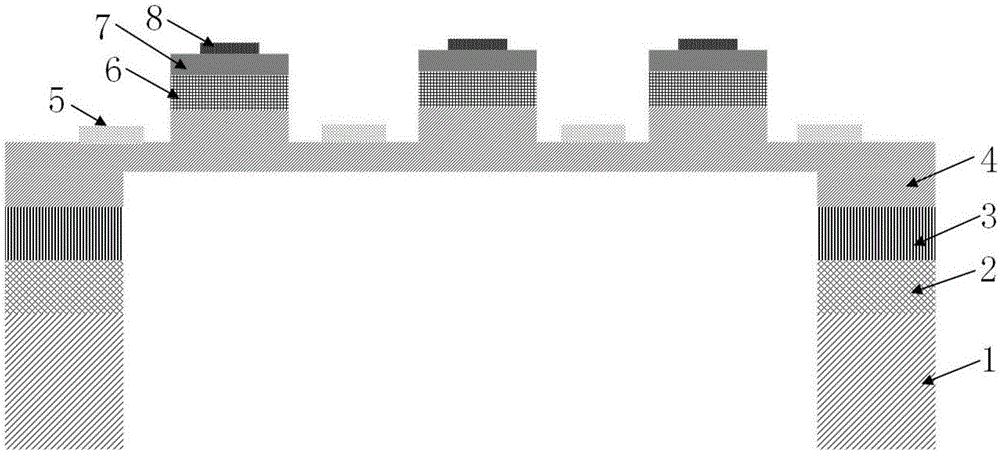
[0023] figure 1 The chip front view of the InGaN-based multi-dimensional visible light communication of the present invention is given. The chip is based on a silicon-based nitride material, and from bottom to top is a silicon substrate layer 1, an epitaxial buffer layer 2, a pure GaN layer 3, an n-electrode 5, and a floating p-n junction quantum well device; the p-n junction quantum well The device includes an n-GaN layer 4, an InGaN / GaN multiple quantum well 6, a p-GaN layer 7, and a p-electrode 8 from bottom to top. There is an etched stepped mesa on the upper surface of the n-GaN layer 4, the stepped mesa includes a lower mesa and an upper mesa, the n-electrode 5 is arranged on the lower mesa, and the upper mesa is more The bottom surfaces of the quantum wells 6 are connected; after the n-GaN layer 4 is peeled off through the back substrate layer 1 and thinned,...


PUM


Abstract

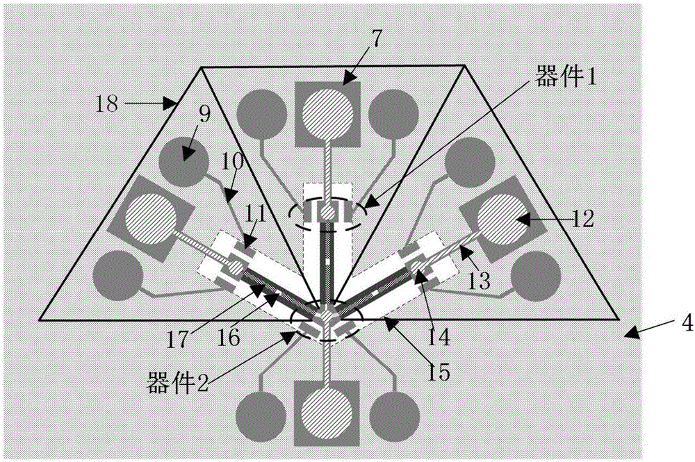
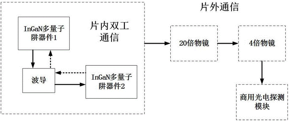
The invention discloses an InGaN photon monolithic integration based multi-dimensional space visible light communication system, which is characterized in that an InGaN photonic integrated circuit of the system is composed of four InGaN multi-quantum well devices and three waveguides; emitted light of the InGaN multi-quantum well devices can be coupled in the chip and can also be transmitted outside the chip, and transmitted optical signals can be detected; and each InGaN multi-quantum well device in the integrated chip not only can act as a light emitting source but also can act as a photoelectric detector, wherein light emitted by the InGaN multi-quantum well device is parallel to the plane and transmitted to another multi-quantum well device through coupling of the waveguides, the received optical signals are converted into electric signals, and one-to-many full duplex optical communication within the chip is realized. The light emitted by the devices on the integrated chip is partially coupled to the waveguides, and the rest of the light is spread to the space. The transmitted optical signals are detected by using a commercial photoelectric detector, and the detected signals are in accordance with computer signals. According to the invention, InGaN photon monolithic integration based multi-dimensional space visible light communication is realized, and a foundation is laid for multi-dimensional visible light communication research.

Description

technical field [0001] The invention relates to a multi-dimensional space visible light communication system based on InGaN photon monolithic integration, and belongs to the technical field of visible light communication. Background technique [0002] At present, visible light wireless communication technology (Light Fidelity, Lifi) uses electrical signals to control the high-speed flashing signals invisible to the naked eye sent by light-emitting diodes to transmit information, but there is a problem that reverse communication cannot be performed; existing full-duplex communication systems use frequency Multiplexing or wavelength division multiplexing technologies realize single-channel full-duplex, which occupies more spectrum and spectrum resources. [0003] The InGaN material has good photoelectric effect, higher band gap, larger electron saturation drift velocity, stronger near-breakdown electric field, higher thermal conductivity and thermal stability, and is ideal for...

Claims


Application Information

Patent Timeline
Patent Type & Authority Applications(China)
IPC IPC(8): H01L31/0352H01L31/16H01L31/173H01L33/06H01L33/32
CPCH01L31/165H01L31/035209H01L31/173H01L33/06H01L33/32
Inventor 王永进蒋燕杨永超高绪敏袁佳磊
Owner NANJING UNIV OF POSTS & TELECOMM
Learn More