Complementary nanowire semiconductor device and preparation method thereof

A semiconductor and nanowire technology, applied in the field of complementary nanowire semiconductor devices and their preparation, can solve problems such as affecting the performance of semiconductor devices, and achieve the effects of excellent electrostatic control and high mobility channel

Active Publication Date: 2017-09-12
ZING SEMICON CORP
View PDF4 Cites 0 Cited by
  • Summary
  • Abstract
  • Description
  • Claims
  • Application Information

AI Technical Summary

Problems solved by technology

Although germanium can be gathered towards the center to form germanium nanowires through the subsequent oxidation thermal annealing treatment, due to the high silicon content of the inner core, that is, the low germanium content of the nanowires, this will affect the performance of the formed semiconductor device

Method used


Image

  • Complementary nanowire semiconductor device and preparation method thereof
  • Complementary nanowire semiconductor device and preparation method thereof
  • Complementary nanowire semiconductor device and preparation method thereof

Examples


Embodiment Construction

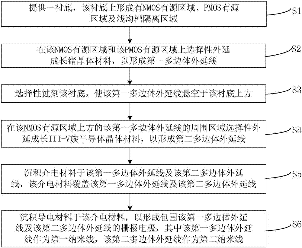
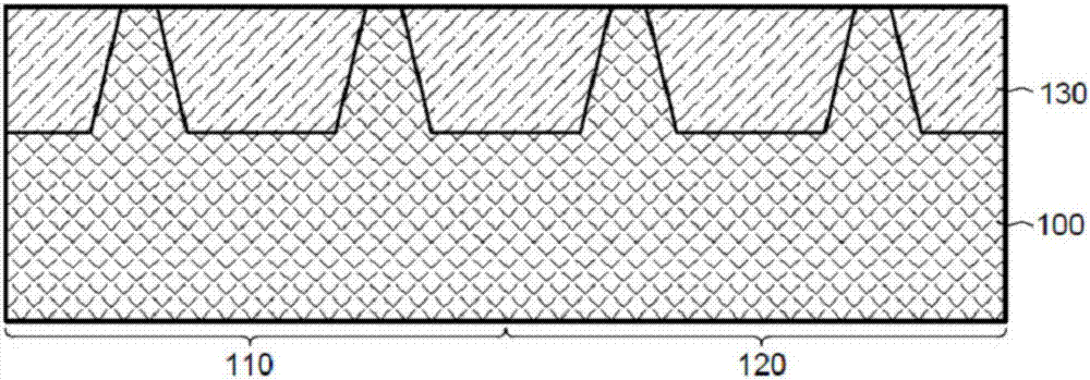
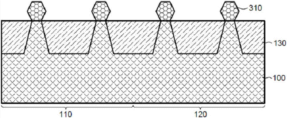
[0029] The complementary nanowire semiconductor device of the present invention and the preparation method thereof will be described in more detail below in conjunction with schematic diagrams, wherein a preferred embodiment of the present invention is represented, it should be understood that those skilled in the art can modify the present invention described here, and still The advantageous effects of the present invention are realized. Therefore, the following description should be understood as the broad knowledge of those skilled in the art, but not as a limitation of the present invention.

[0030] The core idea of ​​the present invention is to provide a complementary nanowire semiconductor device and its preparation method, which has a wrap-around gate surrounding germanium nanowires in the PMOS active region and a wrap-around gate surrounding III-V group in the NMOS active region. nanowires, and the germanium nanowires have a high content of germanium, which can realiz...


PUM


Abstract

The invention provides a complementary nanowire semiconductor device and a preparation method thereof. The preparation method comprises steps of providing a substrate on which an NMOS active region, a PMOS active region, and a shallow trench isolation region are formed; selectively epitaxially growing the germanium crystal material on the NMOS active region and the PMOS active region to form a first polygonal epitaxy; selectively etching the substrate to suspend the first polygonal epitaxial line above the substrate; selectively epitaxially growing Group III-V semiconductor crystalline material in a peripheral region of the first polygonal epitaxy over the NMOS active region to form a second polygonal epitaxy; depositing a dielectric material on the first polygonal epitaxy and the second polygonal epitaxy, wherein the dielectric material covering the first polygonal epitaxy and the second polygonal epitaxy; and depositing a conductive material on the dielectric material to form a gate electrode surrounding the first polygonal epitaxy and the second polygonal epitaxy, wherein the first polygonal epitaxy acting as a first nanowire, and the second polygonal epitaxy acting as a second nanowire.

Description

technical field [0001] The invention relates to the technical field of semiconductor manufacturing, in particular to a complementary nanowire semiconductor device and a preparation method thereof. Background technique [0002] With the continuous innovation of portable electronic products, its process technology is also constantly improving, and the miniaturization of product size is currently the most concerned technology, such as the continuous miniaturization of metal oxide field effect transistors (MOSFET), However, the miniaturization of transistors leads to many physical limitations and problems, such as hot carrier injection, leakage current, insulation, short-channel effects (Short-Channel Effects, SCEs) and channel length control, etc., making the gate of the transistor The ability of the pole to control the channel gradually decreases. [0003] Therefore, in order to solve the problems caused by the miniaturization of transistors, a multi-gate (Multi-Gate) transis...

Claims


Application Information

Patent Timeline
Patent Type & Authority Applications(China)
IPC IPC(8): H01L29/78H01L29/10H01L21/336B82Y10/00
CPCB82Y10/00H01L29/10H01L29/66477H01L29/78H01L21/02639H01L21/8258H01L29/66439H01L29/775H01L29/068H01L29/205H01L21/02532H01L21/02603H01L21/823807H01L27/092H01L29/0673H01L29/42392H01L29/78681H01L29/78684H01L29/78696H01L21/02546H01L21/0262H01L21/02631H01L21/823828H01L21/823878H01L29/0649
Inventor 肖德元
Owner ZING SEMICON CORP
Why Eureka
Try Eureka