Fin field effect transistor and method of forming the same

A fin-type field effect and transistor technology, which is applied in the direction of transistors, semiconductor devices, electric solid-state devices, etc., can solve the problems of increasing the difficulty of the gate structure, and achieve the effect of reducing the difficulty of the process and reducing the process steps

Active Publication Date: 2018-10-16
SEMICON MFG INT (SHANGHAI) CORP
View PDF3 Cites 0 Cited by
  • Summary
  • Abstract
  • Description
  • Claims
  • Application Information

AI Technical Summary

Problems solved by technology

Due to the different materials of the work function layer required by the N-type FinFET and the P-type FinFET, the difficulty of forming the gate structure of the N-type FinFET and the P-type FinFET is further increased.

Method used


Image

  • Fin field effect transistor and method of forming the same
  • Fin field effect transistor and method of forming the same
  • Fin field effect transistor and method of forming the same

Examples


Embodiment Construction

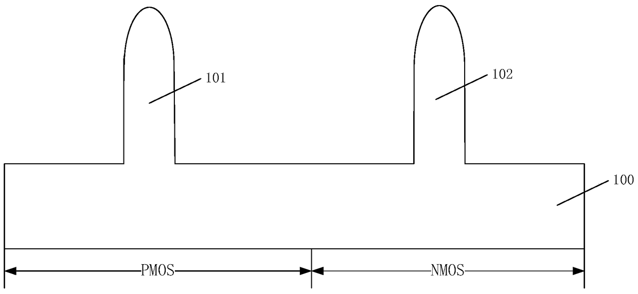
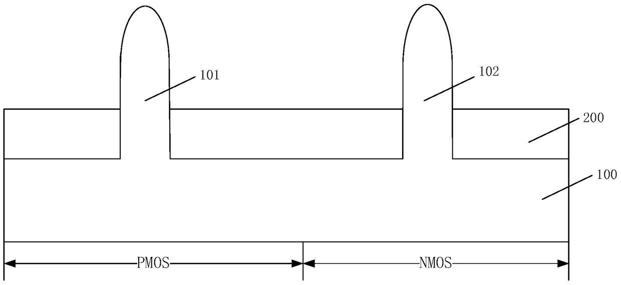
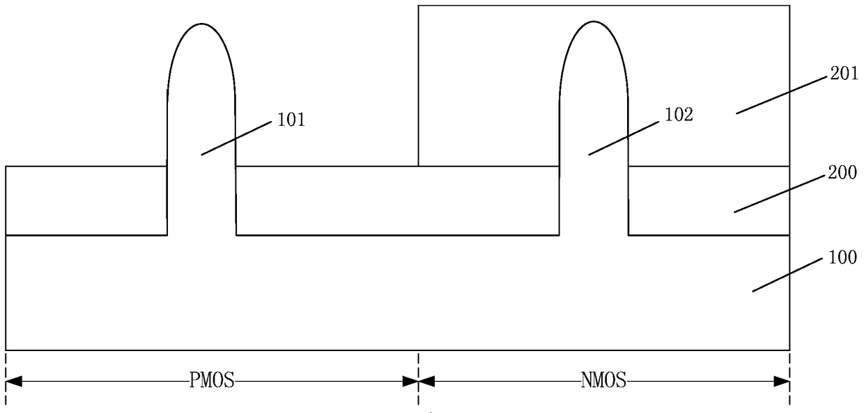
[0031] As mentioned in the background technology, the steps of forming fin field effect transistors in the prior art are relatively complicated. Since the gate work function required by the P-type fin field effect transistor and the N-type fin field effect transistor is different, the P-type fin field effect transistor The fin field effect transistor and the n type fin field effect transistor often need to use work function layers formed of different materials, so that the gate structures of the p type fin field effect transistor and the n type fin field effect transistor need to be formed respectively, which requires more Complicated process steps, and because the fin field effect transistor has a three-dimensional structure, the increase in process steps further increases the difficulty of forming the fin field effect transistor.

[0032] In the embodiment of the present invention, a work function adjustment layer is formed on the first fin of the PMOS region, and the work fu...


PUM


Abstract

Provided is a fin field-effect transistor and a forming method thereof. The fin field-effect transistor forming method comprises: providing a semiconductor substrate including a PMOS region and a NMOS region; forming a first fin portion on the PMOS region and forming a second fin portion on the NMOS region; forming an isolating layer lower than the surface of the first fin portion and the surface of the second fin portion on the surface of the semiconductor substrate; forming a work function adjusting layer on the surface of the first pin portion; simultaneously forming a first gate electrode structure spanning the first fin portion and a second gate electrode structure spanning the second fin portion; and forming a first source electrode and a first drain electrode in the first fin portion on both sides of the first gate electrode structure and forming a second source electrode and a second drain electrode in the second fin portion on both sides of the second gate electrode structure. The above method may reduce the technology difficulty forming the gate electrode structure of the fin field-effect transistor and decrease technology steps.

Description

technical field [0001] The invention relates to the technical field of semiconductors, in particular to a fin field effect transistor and a forming method thereof. Background technique [0002] With the continuous development of semiconductor process technology, the process node is gradually reduced, and the gate-last (gate-last) process has been widely used to obtain an ideal threshold voltage and improve device performance. However, when the feature size of the device is further reduced, even if the gate-last process is adopted, the structure of the conventional MOS field effect transistor can no longer meet the requirements for device performance. Fin field effect transistor (Fin FET) is obtained as a multi-gate device. received widespread attention. [0003] Since N-type FinFET and P-type FinFET have different requirements on gate work function, the gate work function required by P-type FinFET is greater than that required by N-type FinFET. Work function, usually need ...

Claims


Application Information

Patent Timeline
Patent Type & Authority Patents(China)
IPC IPC(8): H01L21/8238H01L21/28H01L27/092H01L29/423H01L29/49
CPCH01L21/823821H01L27/0922H01L27/0924H01L29/401H01L29/42356
Inventor 居建华俞少峰
Owner SEMICON MFG INT (SHANGHAI) CORP
Why Eureka
Try Eureka