
Ge-Cu-Te nano phase change thin film material for high stability phase change random access memory and preparation method thereof

A phase-change memory and thin-film material technology, applied in the field of materials in the field of microelectronics, can solve the problems of poor thermal stability and high operating conversion power consumption, and achieve improved amorphous thermal stability, reduced power consumption, and thermal stability. Sex-enhancing effect

Inactive Publication Date: 2017-08-25
JIANGSU UNIV OF TECH
View PDF8 Cites 2 Cited by
  • Summary
  • Abstract
  • Description
  • Claims
  • Application Information

AI Technical Summary

Problems solved by technology

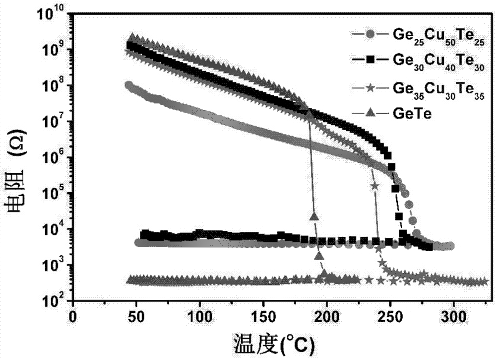
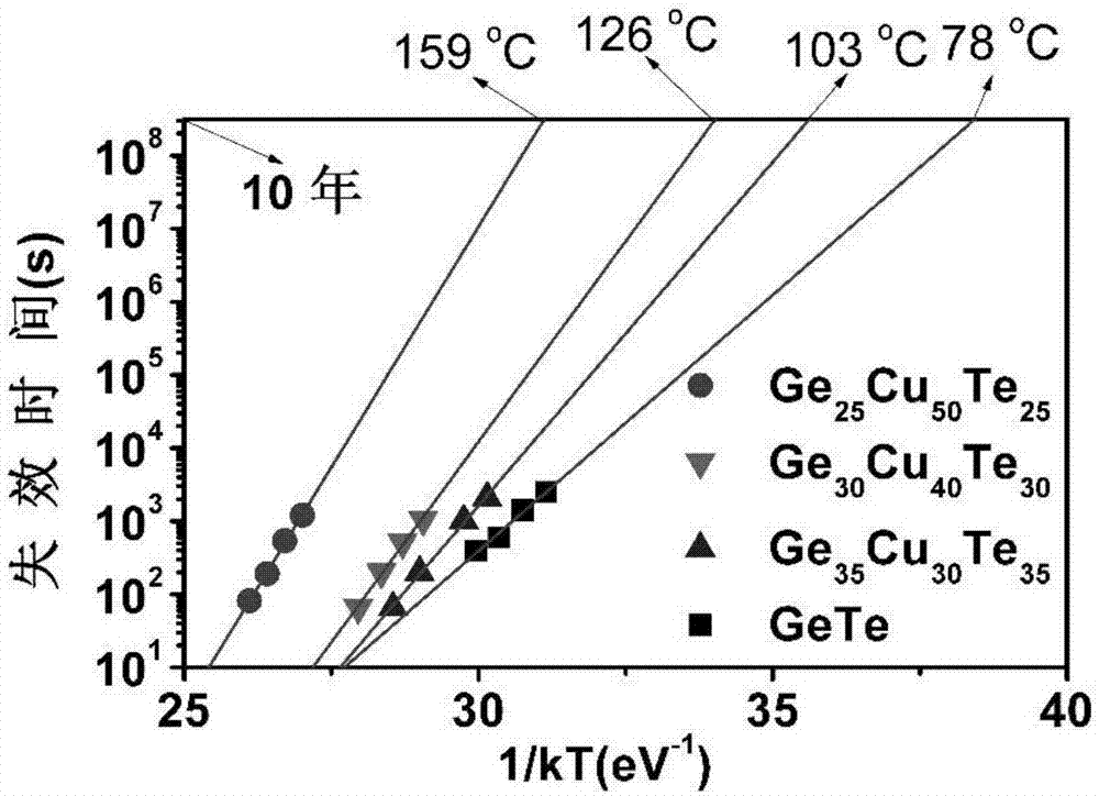
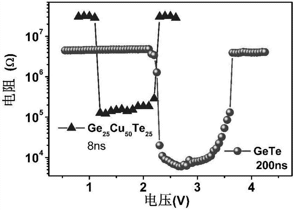
[0005] The purpose of the present invention is to overcome the disadvantages of poor thermal stability of phase change materials in the prior art and high power consumption for operation conversion, and provide a Ge-Cu-Te nano phase change thin film material and its preparation method and application

Method used


Image

  • Ge-Cu-Te nano phase change thin film material for high stability phase change random access memory and preparation method thereof
  • Ge-Cu-Te nano phase change thin film material for high stability phase change random access memory and preparation method thereof
  • Ge-Cu-Te nano phase change thin film material for high stability phase change random access memory and preparation method thereof

Examples


Embodiment 1

[0035] The atomic percentage composition of the Ge-Cu-Te nano phase change film material prepared in this embodiment is Ge 35 Cu 30 Te 35 .

[0036] The preparation steps are:

[0037] 1. Clean SiO2 2 / Si(100) substrate, cleaning the surface and back, removing dust particles, organic and inorganic impurities;

[0038] a) strong ultrasonic cleaning in acetone solution for 10 minutes, and rinse with deionized water;

[0039] b) Strong ultrasonic cleaning in ethanol solution for 10 minutes, rinse with deionized water, high-purity N 2 Blow dry the surface and back;

[0040] c) Dry the water vapor in an oven at 200°C for about 30 minutes.

[0041] 2. Preparation of Ge by RF sputtering method 35 Cu 30 Te 35 Pre-thin film preparation, that is, install the GeTe sputtering target and the composite target Ge x Cu 100-2x Te x ;Set the sputtering power, set the sputtering Ar gas flow and sputtering pressure;:

[0042] a) Install the GeTe sputtering target, stack a circular p...

Embodiment 2

[0050] The atomic percent composition of the film prepared in this embodiment is Ge 30 Cu 40 Te 30 、 Ge 25 Cu 50 Te 25 , the specific preparation process is similar to Example 1, the difference is that the diameter of the Cu target is different, and the preparation of Ge 30 Cu 40 Te 30 The diameter of the Cu target used was 30 mm, and the Ge 25 Cu 50 Te 25 The diameter of the Cu target material used is 40 mm.


PUM

PropertyMeasurementUnit
Thicknessaaaaaaaaaa
Crystallization temperatureaaaaaaaaaa

Abstract

The invention relates to a material in the field of microelectronic technology, and more particularly to a Ge-Cu-Te nano phase change thin film material for a high stability phase change random access memory and a preparation method thereof. The Ge-Cu-Te nano phase change thin film material has an atomic percent composition of GexCu100-2xTex. The Ge-Cu-Te nano phase change thin film material is prepared by depositing a composite target material composed of a GeTe target and a circular pure Cu chip by a high vacuum magnetron sputtering method. The nano phase change thin film material of the invention has high crystallization temperature, which can greatly improve the amorphous thermal stability of the PCRAM; and has high crystal resistance, which can reduce the power consumption of PCRAM.

Description

technical field [0001] The invention relates to a material in the technical field of microelectronics, in particular to a Ge-Cu-Te nanometer phase-change thin film material used for a high-stability phase-change memory and a preparation method thereof. Background technique [0002] Phase-change memory (PCRAM) is a new type of non-volatile memory, which uses chalcogenide materials to achieve information storage by using different high and low resistance values ​​when they undergo rapid phase transitions between crystalline and amorphous states. When different electrical pulses are applied, repeated reversible transitions between the high-resistance state and the low-resistance state can be achieved, achieving the purpose of information storage. Compared with the widely used Flash memory, PCRAM has the advantages of high storage density, low power consumption, fast reading speed, and compatibility with traditional CMOS technology, so it has attracted more and more researchers'...

Claims


Application Information

Patent Timeline
IPC IPC(8): H01L45/00B82Y30/00
CPCB82Y30/00H10N70/026H10N70/8828
Inventor 胡益丰朱小芹尤海鹏邹华袁丽张剑豪吴世臣
Owner JIANGSU UNIV OF TECH
Learn More