Sheets for semiconductor processing
A technology for semiconductors and sheets, applied in the field of sheet materials for semiconductor processing, can solve problems such as seepage and contamination of semiconductor wafers or chip surfaces, and achieve the effect of suppressing pollution and fully antistatic
- Summary
- Abstract
- Description
- Claims
- Application Information
AI Technical Summary
Problems solved by technology
Method used
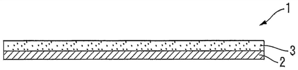
Image

Examples
Embodiment 1
[0160] (1) Preparation of acrylic polymer
[0161] Acrylic polymer (A1) was prepared by copolymerizing 85 parts by mass of n-butyl acrylate and 15 parts by mass of 2-hydroxyethyl acrylate. When the molecular weight of this acrylic polymer (A1) was measured by the method mentioned later, it was 600,000 in weight average molecular weight. The solid content concentration of the obtained acrylic polymer (A1) was diluted to 34 mass % with the mixed solvent of toluene and ethyl acetate.
[0162] (2) Preparation of energy ray curable antistatic polymer (C)
[0163] [2-(methacryloyloxy)ethyl]trimethylammonium bis(trifluoromethanesulfonyl)imide as a quaternary ammonium salt monomer (C1), and a reactive functional group-containing monomer (C2) methacrylic acid, and 2-ethylhexyl acrylate and 2-hydroxyethyl acrylate as polymerizable monomers (C4) become quaternary ammonium salt monomer (C1): methacrylic acid (C2): acrylic acid in molar ratio 2-ethylhexyl ester (C4): 2-hydroxyethyl acry...
Embodiment 2
[0168] [2-(methacryloyloxy)ethyl]trimethylammonium bis(trifluoromethanesulfonyl)imide as a quaternary ammonium salt monomer (C1), and a reactive functional group-containing monomer (C2) Methacrylic acid, methoxypolyethylene glycol acrylate (repeating number of ethylene glycol units: 23) as an ether bond-containing monomer (C3), and 2-ethyl acrylic acid as a polymerizable monomer (C4) Hexyl ester and 2-hydroxyethyl acrylate to become quaternary ammonium salt monomer (C1): methacrylic acid (C2): ether bond monomer (C3): 2-ethylhexyl acrylate (C4): acrylic acid 2 -Hydroxyethyl ester (C4)=0.027:0.015:0.037:0.011:0.011 mode copolymerization. The obtained polymer was reacted with glycidyl methacrylate (0.012 in terms of molar ratio) as a curable group-containing compound (C5) to obtain an energy ray-curable antistatic polymer (C) ( It has methacryloyl, quaternary ammonium salt and ethylene glycol units in the side chain.). The molecular weight of this energy ray-curable antistatic...
Embodiment 3
[0171] An acrylic polymer was prepared by copolymerizing 85 parts by mass of n-butyl acrylate and 15 parts by mass of 2-hydroxyethyl acrylate. When the molecular weight of this acrylic polymer was measured by the method mentioned later, the weight average molecular weight was 500,000. The obtained acrylic polymer was reacted with methacryloyloxyethyl acrylate in an amount of 80 mol% of 2-hydroxyethyl acrylate to obtain an acrylic acid having an energy-ray-curable group introduced into the side chain. Polymer-like (A3).
[0172] Mix 100 parts by mass of the obtained acrylic copolymer (A3), 25 parts by mass of tetraethylene glycol diacrylate as the energy ray curable compound (B) containing an ether bond, and the energy ray curable compound obtained in Example 1. 16 parts by mass of antistatic polymer (C), 3.0 parts by mass of 1-hydroxycyclohexyl phenyl ketone (manufactured by BASF Corporation, Irgacure 184) as a photopolymerization initiator, and toluene diisocyanate compound ...
PUM
| Property | Measurement | Unit |
|---|---|---|
| tensile stress | aaaaa | aaaaa |
| tensile stress | aaaaa | aaaaa |
| wavelength | aaaaa | aaaaa |
Abstract
Description
Claims
Application Information
 - R&D
- Intellectual Property
- Life Sciences
- Materials
- Tech Scout
- Unparalleled Data Quality
- Higher Quality Content
- 60% Fewer Hallucinations
Browse by: Latest US Patents, China's latest patents, Technical Efficacy Thesaurus, Application Domain, Technology Topic, Popular Technical Reports.
© 2025 PatSnap. All rights reserved.Legal|Privacy policy|Modern Slavery Act Transparency Statement|Sitemap|About US| Contact US: help@patsnap.com