


Quick Research
Generate reliable direction feasibility study reports for your R&D in just a few steps.

Technical Q&A
Discover and master advanced knowledge NOW. Basics, ideas, possibilities, all at once.

Find Solutions
As an expert in R&D theories, this can generate solutions to your technical problems instantly.

Evaluate Feasibility
Analyze your overall solution with one click, know your potential R&D risks in advance.

Monitor Landscape
Get weekly tech updates, stay abreast of the latest tech innovations and key insights.
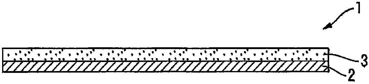
Sheets for semiconductor processing
A technology for semiconductors and sheets, applied in the field of sheet materials for semiconductor processing, can solve the problems of contamination of semiconductor wafers or chips, seepage, etc., and achieve the effect of sufficient antistatic properties and inhibiting pollution
- Summary
- Abstract
- Description
- Claims
- Application Information
AI Technical Summary
Problems solved by technology
Method used
Image

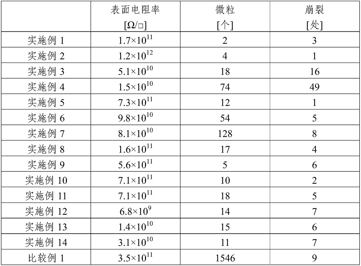
Examples
Embodiment 1
[0135] (1) Preparation of acrylic polymer
[0136] Acrylic polymer (A1) was prepared by copolymerizing 90 parts by mass of n-butyl acrylate and 10 parts by mass of acrylic acid. When the molecular weight of this acrylic polymer (A1) was measured by the method mentioned later, it was 600,000 in weight average molecular weight. The obtained acrylic polymer (A1) was diluted with a mixed solvent of toluene and ethyl acetate to a solid content concentration of 34% by mass.
[0137] (2) Preparation of energy ray curable antistatic polymer (B)
[0138] 45 parts by mass of [2-(methacryloyloxy) ethyl] trimethylammonium bis(trifluoromethanesulfonyl)imide as a quaternary ammonium salt monomer (B1), and 45 parts by mass as a reactive functional group-containing monomer (B2 ) and 5 parts by mass of methacrylic acid, 38 parts by mass of 2-ethylhexyl acrylate and 5 parts by mass of 2-hydroxyethyl acrylate as the polymerizable monomer (B3) were copolymerized. 7 parts by mass of glycidyl me...
Embodiment 2
[0143] In the said process (3), except having changed the addition amount of the energy ray curable antistatic polymer (B) to 1.5 mass parts, it carried out similarly to Example 1, and manufactured the sheet|seat for semiconductor processing.
Embodiment 3
[0145] In the said process (3), except having changed the addition amount of the energy ray curable antistatic polymer (B) into 100 mass parts, it carried out similarly to Example 1, and manufactured the sheet|seat for semiconductor processing.
PUM
| Property | Measurement | Unit |
|---|---|---|
| tensile stress | aaaaa | aaaaa |
| transition temperature | aaaaa | aaaaa |
| wavelength | aaaaa | aaaaa |
Abstract
Description
Claims
Application Information
 - R&D Engineer
- R&D Manager
- IP Professional
- Industry Leading Data Capabilities
- Powerful AI technology
- Patent DNA Extraction
Browse by: Latest US Patents, China's latest patents, Technical Efficacy Thesaurus, Application Domain, Technology Topic, Popular Technical Reports.
© 2024 PatSnap. All rights reserved.Legal|Privacy policy|Modern Slavery Act Transparency Statement|Sitemap|About US| Contact US: help@patsnap.com