Manufacture method for subsided high-density mutual connection board

A manufacturing method and technology of flexible boards, which are applied in multilayer circuit manufacturing, printed circuit manufacturing, printed circuit and other directions, can solve the problems of unsatisfactory fineness, inability to etch, difficult to etch, etc. The effect of dimensional stability and improved bonding force

Active Publication Date: 2017-07-18
NINGBO HUAYUAN ELECTRONICS TECH
View PDF7 Cites 9 Cited by
  • Summary
  • Abstract
  • Description
  • Claims
  • Application Information

AI Technical Summary

Problems solved by technology

This kind of soft-rigid circuit board is prepared by metal welding and interconnection. Metal welding columns are used to replace the original mechanical drilling or laser drilling. The minimum diameter can be 0.05mm, which increases the area where the design can be routed, but The production of the outer layer circuit adopts the ordinary etching (subtraction) process, and the ordinary etching (subtraction) process makes the circuit: the minimum line width is about 50\50um, and the thicker the copper thickness, the harder it is to etch the line, and the larger the etched burrs, When the copper thickness exceeds 20um, the line width of 50\50um cannot be etched
Therefore, the method of metal welding and interconnection is not ideal in terms of fine line production, so the production process needs to be improved and optimized.

Method used


Image

  • Manufacture method for subsided high-density mutual connection board
  • Manufacture method for subsided high-density mutual connection board
  • Manufacture method for subsided high-density mutual connection board

Examples


Embodiment Construction

[0034] The present invention will be further described in detail below in conjunction with the accompanying drawings and embodiments.

[0035] Such as Figure 1-10 as shown,

[0036] The manufacturing method of the rigid-flex circuit board of the present embodiment, its technological process is:

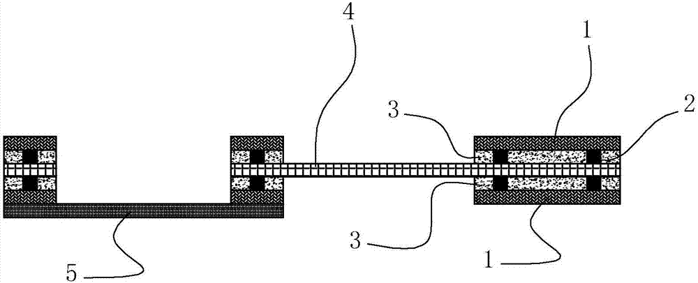
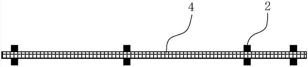
[0037] Normal production of inner soft board 4—conduction copper pillar 2 electroplating—insulation adhesive layer 3 lamination—insulation adhesive layer 3 grinding—outer hard board 1 circuit formation (additive electroplating process)—— Subsidence area 6 processing - steel plate 5 processing

[0038] Specifically include the following steps:

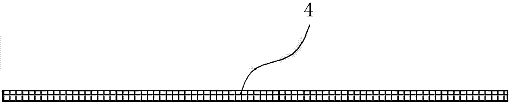
[0039] 1) Make the inner soft board 4 (such as figure 2 ), the inner flexible board 4 is produced by conventional methods, specifically including: first cutting the inner soft board 4, drilling and electroplating conduction, the drilling can be mechanical drilling or laser drilling, and then the inner layer Etching of 4 lines on the flex...


PUM


Abstract

A manufacture method for a subsided high-density mutual connection board includes steps of manufacturing an inner layer soft board; manufacturing conducting copper posts in conduction with an outer layer rigid board by utilizing an addition process on the upper side and the lower side of the inner layer soft board or on one side of the inner layer soft board and performing electroplating on the conducting copper posts; filling an insulation bonding layer bonded with the outer layer rigid board on the upper side and the lower side of the inner layer soft board or on the same side of the inner layer soft board and grinding the surface of the insulation bonding layer so as to expose the conducting copper posts; manufacturing an outer layer rigid board circuit by adopting an addition process electroplating technology on the insulation bonding layer; performing hollowing processing on a subsided region; and performing steel board reinforcement processing on the bottom part of the subsided region. According to the invention, the conducting copper posts manufactured through addition electroplating are adopted to replace traditional drilling holes and laser drilling holes for conduction; the minimum diameter of each conducting copper post can be as small as 0.05 mm; wiring can be performed on the conducting posts and the minimum wire width\wire space of the circuit manufactured by using the addition process can be 15\15 micrometers. Therefore, circuit fineness is improved and wiring density is improved substantially. The invention also has characteristics of simple manufacture process and low cost and area available for wiring is enlarged.

Description

technical field [0001] The invention relates to the technical field of printed circuit board manufacturing, in particular to a method for manufacturing a sunken high-density interconnection board. Background technique [0002] With the continuous advancement of technology, the functional requirements of electronic products are getting higher and higher. At the same time, the appearance is also very short, small, light and thin. For this reason, more and more circuit boards with multi-layer integrated functions are used, especially It is the high-density interconnection board that has developed rapidly in recent years. High-density interconnection board is a high-precision, thin-line, small-aperture, ultra-thin printed board. It introduces blind buried holes in conventional circuit boards, fine line width and line spacing, and can manufacture conventional multi-layer board technology. Thin, multi-layer, stable circuit boards that cannot be achieved, which have the following ...

Claims


Application Information

Patent Timeline
Patent Type & Authority Applications(China)
IPC IPC(8): H05K3/46
CPCH05K1/111H05K3/4614H05K2201/09663
Inventor 张成立王强
Owner NINGBO HUAYUAN ELECTRONICS TECH
Why Eureka
Try Eureka