Silicon epitaxial wafer and its preparation method

A technology of silicon epitaxial wafers and epitaxial layers, which is applied in the manufacture of semiconductor/solid-state devices, semiconductor devices, electrical components, etc., can solve the problems of difficult overlapping of the center and edge transition regions, and the large influence of self-doping effects, so as to improve the softness factor, maintaining electrical characteristics, and the effects of controllable linear distribution parameters

Active Publication Date: 2020-12-15
HEBEI POSHING ELECTRONICS TECH
View PDF4 Cites 0 Cited by
  • Summary
  • Abstract
  • Description
  • Claims
  • Application Information

AI Technical Summary

Problems solved by technology

[0009] Another non-traditional process uses the simultaneous gradient (Ramp) method of injection and dilution flow rate. Through precise control of the flow rate, a long transition region epitaxial layer with a controllable epitaxial concentration gradient can be formed. After the growth of the transition region is completed, use The outermost N-layer is grown by the traditional process to maintain the electrical parameter characteristics such as the reverse voltage required by the device. The disadvantage is that the epitaxial transition region with a low resistance value of 0.05-1ohm.cm in the first layer has a great influence on the self-doping effect of the system. It is difficult to coincide with the edge transition zone

Method used


Image

  • Silicon epitaxial wafer and its preparation method
  • Silicon epitaxial wafer and its preparation method
  • Silicon epitaxial wafer and its preparation method

Examples


Embodiment 1

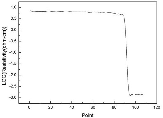
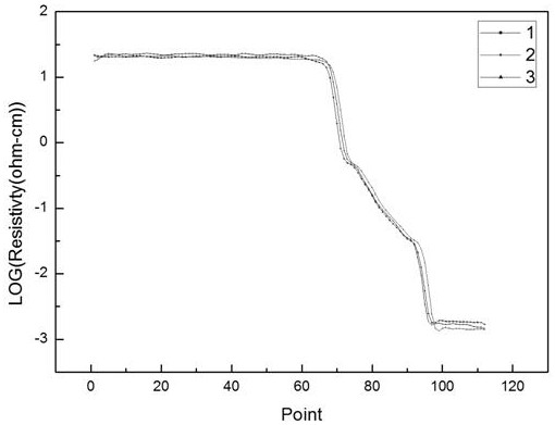
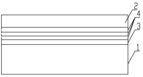
[0035] The embodiment of the present invention discloses a silicon epitaxial wafer, such as image 3 As shown, the epitaxial wafer includes a silicon substrate 1, the inner epitaxial layer is located on the upper surface of the substrate, and the high resistance epitaxial layer 2 is located on the upper surface of the inner epitaxial layer; the inner epitaxial layer includes The low-resistance epitaxial layer 3 on the lower side and more than two linear graded epitaxial layers 4 on the upper surface of the low-resistance epitaxial layer 3 .

[0036] Preferably, the silicon epitaxial wafer meets the following parameters: the silicon substrate 1 uses an N-type polished wafer heavily doped with arsenic. The thickness of the low-resistance epitaxial layer 3 is 0.5 μm-2 μm, and the resistivity is 0.5Ω.cm-10Ω.cm. The thickness of the linear graded epitaxial layer 4 of the single layer is 5 μm-10 μm, the first to nth linear graded epitaxial layers are arranged from bottom to top, t...

Embodiment 2

[0039] The main equipment used in the method of the present invention is an Italian PE-3061D epitaxial furnace, and the base is a high-purity graphite base.

[0040] Such as Figure 4 As shown, the present invention also discloses a method for preparing a silicon epitaxial wafer, the method comprising the steps of:

[0041] S101: directly growing a low-resistance epitaxial layer 3 on the upper surface of the silicon substrate 1;

[0042] S102: growing a layer of linear graded epitaxial layer 4 every 5 μm-10 μm on the upper surface of the low-resistance epitaxial layer 3, and calculating the doping flux corresponding to the linear resistance value of the graded epitaxial layer during growth for doping;

[0043] S103: growing a high-resistance epitaxial layer 2 on the upper surface of the outermost linear graded epitaxial layer 4 .

Embodiment 3

[0045] The main equipment used in the method of the present invention is an Italian PE-3061D epitaxial furnace, and the base is a high-purity graphite base.

[0046] Such as Figure 5 As shown, the present invention also discloses a method for preparing a silicon epitaxial wafer, the method comprising the steps of:

[0047] S201: Treatment of the epitaxial furnace: before loading the silicon substrate, the reaction chamber of the epitaxial furnace is thoroughly treated with HCl at high temperature to ensure the purity of the chamber, and then the graphite base is coated with silicon.

[0048] S202: Wafer pretreatment: using H 2 The natural oxide layer of the silicon substrate is baked to reduce the self-doping effect and ensure the consistency of resistivity in the chip.

[0049] S203: Epitaxial layer growth: the first layer grows a low-resistance epitaxial layer with a thickness of 0.5 microns-2 microns and a resistivity of 0.5 ohm.cm-1ohm.cm, and then grows more than two l...


PUM

PropertyMeasurementUnit
thicknessaaaaaaaaaa
electrical resistivityaaaaaaaaaa
thicknessaaaaaaaaaa

Abstract

The invention discloses a silicon epitaxial wafer and a preparation method thereof, and relates to the technical field of manufacturing or processing methods of semiconductor devices. The preparation method comprises the following steps: directly growing a low-resistance epitaxial layer on the upper surface of a silicon substrate; growing a linear gradient epitaxial layer every 5-10 microns on the upper surface of the low-resistance epitaxial layer, calculating a doping flow rate corresponding to a linear resistance value of the gradient epitaxial layer for doping during growing; and growing a high-resistance epitaxial layer on the upper surface of an outermost linear gradient epitaxial layer. An inner layer epitaxial layer of the epitaxial wafer provided by the invention comprises two or more linear gradient epitaxial layers; the linear gradient epitaxial layer adopts multi-layer growth; and a small amount of dopant among layers preferentially enters a reaction chamber to change an epitaxial growth environment. Meanwhile, by using a simultaneously gradient flow rate method (namely, a ramp method), not only is a softness factor of the device improved, but also original electric characteristics of the device are kept, so that a controllable linear distribution parameter of a transition zone is totally realized, and the repeatability and the consistency are high.

Description

technical field [0001] The invention relates to the technical field of manufacturing or processing methods of semiconductor devices, in particular to a silicon epitaxial wafer and a preparation method thereof. Background technique [0002] Under the forward bias voltage, the conduction resistance of the PIN structure diode is very small, which is close to a short circuit; under the reverse bias voltage, the impedance is very high, close to an open circuit; and it has the characteristics of large power capacity, small loss, fast speed, etc., so in Widely used in power diodes. For example: In electronic circuits such as switching power supplies, PWM pulse width modulators, and frequency converters, they are used as high-frequency rectifier diodes, freewheeling diodes, or damping diodes. [0003] With the continuous development of electronic technology and integrated circuits, higher requirements are put forward for the stability and reliability of power semiconductor devices....

Claims


Application Information

Patent Timeline
Patent Type & Authority Patents(China)
IPC IPC(8): H01L29/868H01L29/06H01L21/329
CPCH01L29/0684H01L29/6609H01L29/868
Inventor 高国智陈秉克赵丽霞袁肇耿薛宏伟吴会旺张绪刚
Owner HEBEI POSHING ELECTRONICS TECH
Why Eureka
Try Eureka