Diode chip structure and preparation method thereof

A chip structure and diode technology, applied in semiconductor/solid-state device manufacturing, electrical components, circuits, etc., can solve problems such as large overshoot voltage, poor diode softness, and damage to system circuit components, to improve withstand voltage capability, reduce Reverse leakage current, the effect of slowing down the reverse pumping speed

Pending Publication Date: 2021-08-06
CHINA ZHENHUA GRP YONGGUANG ELECTRONICS CO LTD STATE OWNED NO 873 FACTORY
View PDF0 Cites 0 Cited by
  • Summary
  • Abstract
  • Description
  • Claims
  • Application Information

AI Technical Summary

Problems solved by technology

[0004] When the above-mentioned diode is in forward conduction, a large number of minority carrier holes and electrons are stored in the lightly doped N-drift region and the heavily doped P+ region. When the device is turned off, its depletion region is lightly doped The N-drift region and the heavily doped P+ region expand outward; due to the lower concentration on the side of the lightly doped N-drift region, the depletion region mainly expands to the side of the lightly doped N-drift region; in the depletion region In the process of expansion, the minority carriers in the area passed by the depletion region are quickly swept out, causing the reverse recovery current to rapidly decrease to zero, making the fast recovery diode softer, resulting in a large overshoot voltage in the loop , causing damage to system circuit components

Method used


Image

  • Diode chip structure and preparation method thereof
  • Diode chip structure and preparation method thereof
  • Diode chip structure and preparation method thereof

Examples


Embodiment 1

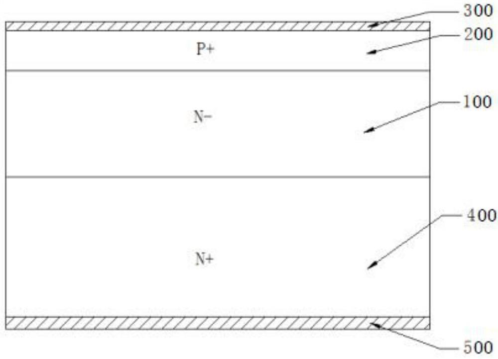
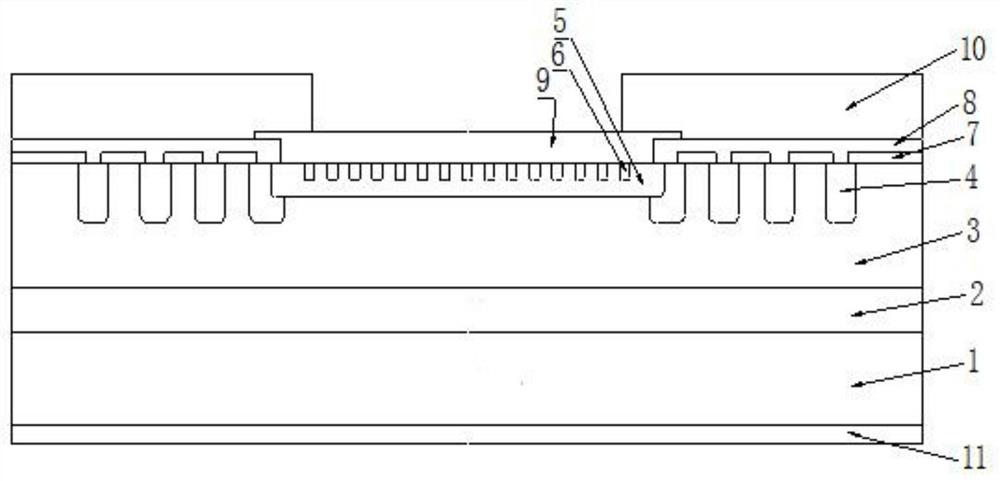
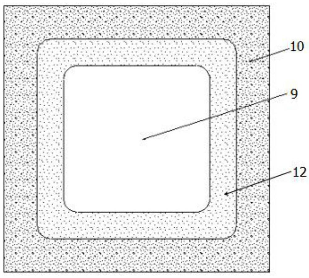
[0049] An embodiment of the present invention provides a diode chip structure, such as figure 2 As shown, a double-base structure is adopted, including an N+ substrate 1 and an N buffer layer 2 and an N- epitaxial region 3 that are sequentially grown on top of it; 4. The central area in the top of the N- epitaxial region 3 is the P base region 5, the P base region 5 is periodically inlaid with the active P+ region 6, the metallized anode 9 is made on the top of the P base region 5, and the oxidation is made on the top of the P+ring region 4 The top of silicon 7 and silicon oxide 7 passivates borophosphosilicate glass 8 , and borophosphosilicate glass 8 is covered by silicon nitride 10 , and the back of N+ substrate 1 is a metallized cathode 11 .

[0050] Among them, the metallized anode is an aluminum electrode with a thickness of 3-4um, and the metallized cathode is a titanium, nickel or silver electrode with a thickness of 0.1±0.01um / 0.6±0.1um / 0.8±0.1um respectively.

[00...


PUM

PropertyMeasurementUnit
electrical resistivityaaaaaaaaaa

Abstract

The invention discloses a diode chip structure and a preparation method thereof. The diode comprises an N + substrate, and an N buffer layer and an N- epitaxial region which are sequentially stacked and grown on the top of the N + substrate; a P + ring region is embedded at the outer end of the top of the N- epitaxial region, a central region in the top of the N- epitaxial region is a P base region, an active P + region is periodically embedded in the P base region, a metalized anode is manufactured at the top of the P base region, silicon oxide is manufactured at the top of the P + ring region, boron phosphorosilicate glass is passivated at the top of the silicon oxide, the boron phosphorosilicate glass is covered by silicon nitride, and a metalized cathode is arranged on the back surface of the N + substrate. According to the invention, the N buffer layer at the bottom of the N- epitaxial region can buffer the expansion of the space charge region, slow down the reverse extraction speed of carriers, and soften the recovery characteristics. The active P + region is periodically embedded in the P base region, the anode injection efficiency can be remarkably reduced, reverse storage charges are reduced, the reverse recovery time is shortened, a junction terminal is of a floating field limiting ring structure, the voltage endurance capability of the diode is enhanced, and the reverse leakage current of the device is reduced.

Description

technical field [0001] The invention relates to the technical field of semiconductors, in particular to a diode chip structure and a preparation method. Background technique [0002] Fast recovery diodes have the characteristics of good switching characteristics and short reverse recovery time. They are mainly used in electronic circuits such as switching power supplies, PWM pulse width modulators, and frequency converters, as high-frequency rectifier diodes, freewheeling diodes, or damping diodes. [0003] Existing fast recovery diodes such as figure 1 As shown, its structure includes: lightly doped N-drift region 100; heavily doped P+ region 200 on top of lightly doped N-drift region 100; anode metal layer 300 on top of heavily doped P+ region 200; Doping the heavily doped N+ substrate layer 400 at the bottom of the N-type drift region 100 ; and the cathode metal layer 500 at the bottom of the heavily doped N+ substrate layer 400 . [0004] When the above-mentioned diode...

Claims


Application Information

Patent Timeline
Patent Type & Authority Applications(China)
IPC IPC(8): H01L29/861H01L29/06H01L21/329
CPCH01L29/0619H01L29/66136H01L29/861
Inventor 贺晓金袁强陆超姚秋原孟繁新王博洪杜桥
Owner CHINA ZHENHUA GRP YONGGUANG ELECTRONICS CO LTD STATE OWNED NO 873 FACTORY
Why Eureka
Try Eureka