A superjunction device with improved body diode characteristics

A body diode and super junction device technology, applied in the direction of semiconductor devices, electrical components, circuits, etc., can solve the problems of high reverse recovery hardness of body diodes, voltage and current overshoot, large electromagnetic interference, etc., to improve EMI characteristics, The effect of alleviating mutation and increasing softness factor

Active Publication Date: 2022-07-08
江苏长晶科技股份有限公司 +1
View PDF5 Cites 0 Cited by
  • Summary
  • Abstract
  • Description
  • Claims
  • Application Information

AI Technical Summary

Problems solved by technology

When the body diode is in the conduction state, a large amount of excess carriers are stored in the N column region, so that the super-junction DMOS has a lot of reverse recovery charges; when the body diode is in the reverse recovery state, due to the large area of ​​the PN junction Many, the extraction of non-equilibrium carriers is accelerated, which causes the body diode of the super-junction DMOS to have a high reverse recovery hardness, which is easy to generate large voltage and current overshoots, resulting in large electromagnetic interference (EMI) noise, and even device damage

Method used


Image

  • A superjunction device with improved body diode characteristics
  • A superjunction device with improved body diode characteristics
  • A superjunction device with improved body diode characteristics

Examples


Embodiment 1

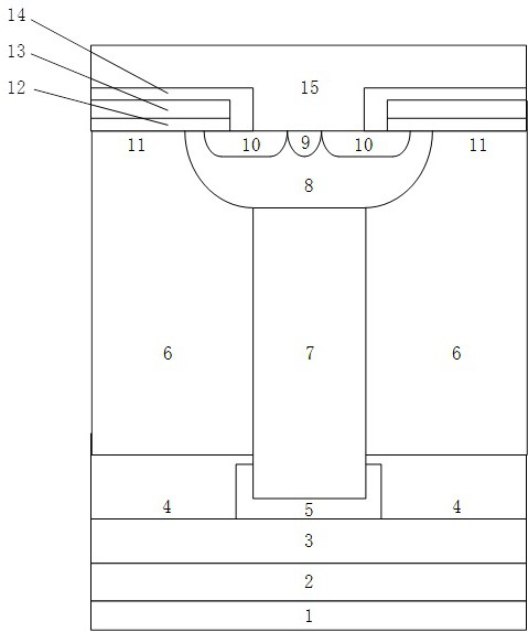
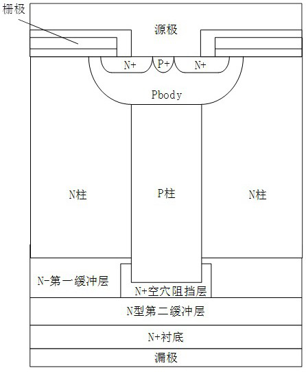
[0015] An N-type superjunction DMOS device with improved body diode characteristics, wherein the first conductive type semiconductor is an N-type semiconductor, and the second conductive type semiconductor is a P-type semiconductor, such as figure 2 As shown, the device has from bottom to top: a metallized drain, a heavily doped N-type substrate over the metallized drain, an N-type second buffer layer over the N+ substrate, an N-type second buffer N-type first buffer layer above the layer; the top of the N-type first buffer layer has an N-type semiconductor epitaxial layer; the N-type semiconductor epitaxial layer has a P-type semiconductor pillar; the top of the P-type semiconductor pillar There is a P-type semiconductor body region; the interior of the P-type semiconductor body region has a heavily doped P+ semiconductor contact region and a heavily doped N+ semiconductor source region, the heavily doped P+ semiconductor contact region and the heavily doped N+ semiconductor ...


PUM


Abstract

A superjunction device with improved body diode characteristics, comprising from bottom to top: a metallized drain, a heavily doped first conductivity type semiconductor substrate, a first conductivity type semiconductor buffer layer and a low doped first conductivity type semiconductor buffer layer , the first conductive type semiconductor epitaxial layer and the second conductive type semiconductor column form a superjunction structure, and the second conductive type semiconductor column extends downward into the low-doped first conductive type semiconductor buffer layer and is highly doped by the first conductive type semiconductor. Surrounded by the type semiconductor barrier layer, the highly doped first conductivity type semiconductor barrier layer is also located in the low doped first conductivity type semiconductor buffer layer. The invention introduces a double buffer layer structure and a barrier layer structure at the bottom of the super junction column, which effectively slows down the unbalanced carrier extraction speed at the bottom of the drift region, thereby reducing the current change rate during the reverse recovery process of the device and alleviating the reverse The sudden change to the current increases the soft factor of the reverse recovery of the body diode and improves the EMI characteristics of the device.

Description

technical field [0001] The present invention relates to the technical field of power semiconductor devices, and relates to a super-junction DMOS device, which is a super-junction device with improved body diode characteristics. Background technique [0002] Due to its unique high input impedance, low driving power, high switching speed, superior frequency characteristics, and good thermal stability, power DMOS is widely used in switching power supplies, automotive electronics, motor drives and other fields. Super-junction (Super-junction) DMOS device is an important power device that has appeared in recent years. Its basic principle is the principle of charge balance. By introducing super-spaced P-pillars and N-pillars in the drift region of ordinary power DMOS. The junction structure greatly improves the trade-off relationship between the on-resistance and the breakdown voltage of ordinary DMOS, so it has been widely used in power systems. [0003] Superjunction DMOS has a...

Claims


Application Information

Patent Timeline
Patent Type & Authority Patents(China)
IPC IPC(8): H01L29/06H01L29/78
CPCH01L29/7802H01L29/0684
Inventor 杨国江于世珩
Owner 江苏长晶科技股份有限公司
Why Eureka
Try Eureka