


Quick Research
Generate reliable direction feasibility study reports for your R&D in just a few steps.

Technical Q&A
Discover and master advanced knowledge NOW. Basics, ideas, possibilities, all at once.

Find Solutions
As an expert in R&D theories, this can generate solutions to your technical problems instantly.

Evaluate Feasibility
Analyze your overall solution with one click, know your potential R&D risks in advance.

Monitor Landscape
Get weekly tech updates, stay abreast of the latest tech innovations and key insights.
Super junction device manufacturing method and device structure
A technology of super junction devices and manufacturing methods, applied in semiconductor/solid-state device manufacturing, semiconductor devices, electrical components, etc., can solve the problems of high production costs, achieve low production costs, and improve the softness factor of reverse recovery.
- Summary
- Abstract
- Description
- Claims
- Application Information
AI Technical Summary
Problems solved by technology
Method used
Image

Examples
no. 1 example approach
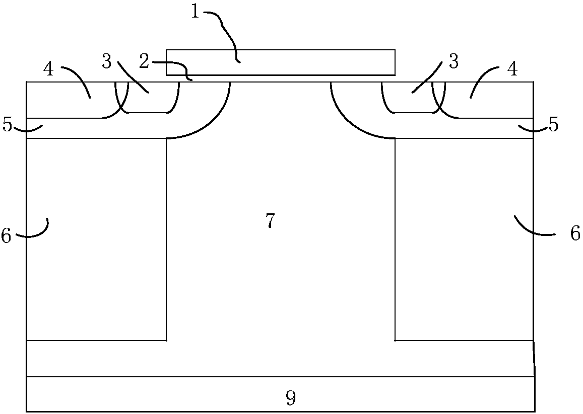
[0057] like Figure 4 Shown is the flow chart of the method of the first embodiment of the present invention; as Figure 5A to Figure 5F As shown, it is a device structure diagram in each step of the method of the first embodiment of the present invention; in the manufacturing method of the super-junction device in the first embodiment of the present invention, an N-type super-junction device is taken as an example for illustration, and the second conductivity type is N-type, the second conductivity type is P-type; comprising the following steps:
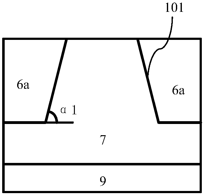
[0058] Step 1, such as Figure 5A As shown, a trench 101 is formed in the N-type epitaxial layer 7 .
[0059] The N-type epitaxial layer 7 is formed on the wafer surface composed of a semiconductor substrate such as a silicon substrate 9 . The semiconductor substrate 9 is N+ doped, and the doping concentration is usually 2e19cm -3 ~2e20cm -3 The corresponding resistivity is between 0.5mohm and 3mohm; the high doping concentrati...
no. 2 example approach
[0080] The difference between the method of the second embodiment of the present invention and the method of the first embodiment of the present invention is:
[0081] like Figure 7 Shown is a device structure diagram formed in the steps of the method of the second embodiment of the present invention. In the method of the second embodiment of the present invention, the side wall ion implantation adopts two N-type ion implantations, mainly because the implantation angle is changed to α 2 , that is, two α 2 .
[0082] Specifically, the N-type doping increased region 203 is formed by N-type ion implantation when α is 11 degrees, which is the same as the method in the first embodiment of the present invention, and the implantation angle of 11 degrees is within 20 μm from the surface. The sidewalls are implanted with N-type impurities.
[0083] The N-type doping increased region 203a is increased once α 2 It is formed by N-type ion implantation at 20 degrees, and at an implan...
no. 3 example approach
[0085] The difference between the method of the third embodiment of the present invention and the method of the first embodiment of the present invention is:
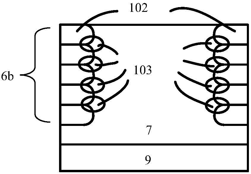
[0086] In the method according to the third embodiment of the present invention, one N-type ion implantation and one P-type ion implantation are used for the sidewall ion implantation.
[0087] The sidewall ion implantation also includes at least one P-type ion implantation, the implantation region corresponding to the P-type ion implantation is located at a certain depth downward from the top surface of the trench 101 and the P-type ion implantation The formula of the implantation region corresponding to the implantation is the same as the formula of the implantation region corresponding to the N-type ion implantation.
[0088] After the implantation region corresponding to the P-type ion implantation is superimposed on the implantation region corresponding to the N-type ion implantation, the N-type doping in the overl...
PUM
| Property | Measurement | Unit |
|---|---|---|
| Width | aaaaa | aaaaa |
Abstract
Description
Claims
Application Information
 - R&D Engineer
- R&D Manager
- IP Professional
- Industry Leading Data Capabilities
- Powerful AI technology
- Patent DNA Extraction
Browse by: Latest US Patents, China's latest patents, Technical Efficacy Thesaurus, Application Domain, Technology Topic, Popular Technical Reports.
© 2024 PatSnap. All rights reserved.Legal|Privacy policy|Modern Slavery Act Transparency Statement|Sitemap|About US| Contact US: help@patsnap.com