Silicon-carbon negative electrode material and preparation method thereof
A technology of negative electrode material and silicon carbon, which is applied to the field of silicon carbon negative electrode material and its preparation, can solve the problems such as the inability to protect the core structure, the fixed nuclear structure, the limited flexibility of the surface coating layer, and the influence on the performance of the silicon carbon negative electrode material. Achieve excellent ion conductivity, electrochemical performance, and tight adhesion
- Summary
- Abstract
- Description
- Claims
- Application Information
AI Technical Summary
Problems solved by technology
Method used
Image
Examples
Embodiment 1
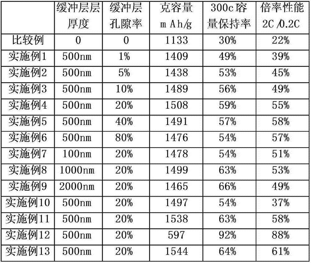
[0036] Embodiment 1, differs from comparative example in that this embodiment comprises the following steps:
[0037] Step 1. Evenly mix 100nm silicon particles, carbon nanotube conductive agent (silicon particle:conductive agent=9:1, mass ratio, the same below), and NMP to obtain a precursor slurry, and then spray and pelletize to obtain a silicon-based secondary particles;
[0038] Step 2. Mix super conductive carbon, glucose, 2-methyl-2-nitrosopropane (accounting for 1% of the volume of the solid component), and NMP to obtain a slurry;
[0039] Step 3. Coat the slurry obtained in step 2 on the surface of the core structure particles described in step 1, and then perform a foaming reaction to obtain a porous structure precursor coating layer, which is then carbonized to obtain a thickness of 500 nm and a porosity of 1%. buffer layer;
[0040] Step 4. Select asphalt as the coating material to coat the product of step 3. Since the product of step 3 has been carbonized, the s...
Embodiment 2
[0042] Embodiment 2 is different from Embodiment 1 in that this embodiment includes the following steps:
[0043] Step 2. Mix super conductive carbon, glucose, 2-methyl-2-nitrosopropane (accounting for 5% of the volume of the solid component), and NMP to obtain a slurry;
[0044] Step 3. Coat the slurry obtained in step 2 on the surface of the core structure particles described in step 1, and then perform a foaming reaction to obtain a porous structure precursor coating layer, which is then carbonized to obtain a thickness of 500 nm and a porosity of 5%. buffer layer;
[0045] Others are the same as in Example 1, and will not be repeated here.
Embodiment 3
[0046] Embodiment 3 is different from Embodiment 1 in that this embodiment includes the following steps:
[0047] Step 2. Mix super conductive carbon, glucose, 2-methyl-2-nitrosopropane (accounting for 10% of the volume of the solid component), and NMP to obtain a slurry;
[0048] Step 3. Coat the slurry obtained in step 2 on the surface of the core structure particles described in step 1, then perform a foaming reaction to obtain a porous structure precursor coating layer, and then carbonize to obtain a thickness of 500nm and a porosity of 10%. buffer layer;
[0049] Others are the same as in Example 1, and will not be repeated here.
PUM
| Property | Measurement | Unit |
|---|---|---|
| diameter | aaaaa | aaaaa |
| thickness | aaaaa | aaaaa |
| thickness | aaaaa | aaaaa |
Abstract
Description
Claims
Application Information
 - R&D
- Intellectual Property
- Life Sciences
- Materials
- Tech Scout
- Unparalleled Data Quality
- Higher Quality Content
- 60% Fewer Hallucinations
Browse by: Latest US Patents, China's latest patents, Technical Efficacy Thesaurus, Application Domain, Technology Topic, Popular Technical Reports.
© 2025 PatSnap. All rights reserved.Legal|Privacy policy|Modern Slavery Act Transparency Statement|Sitemap|About US| Contact US: help@patsnap.com

