
Silicon nanowire-based thin-film silicon crystalline silicon laminated solar photovoltaic cell

A technology of silicon nanowires and photovoltaic cells, applied in photovoltaic power generation, circuits, electrical components, etc., can solve the problems of high purity requirements of amorphous silicon materials, weak photo-generated current of photovoltaic cells, low cell efficiency, etc., and achieve thickness reduction, The effect of high photogenerated voltage and large photocurrent

Inactive Publication Date: 2017-05-31
SHANGHAI DIANJI UNIV
View PDF5 Cites 0 Cited by
  • Summary
  • Abstract
  • Description
  • Claims
  • Application Information

AI Technical Summary

Problems solved by technology

[0004] At present, the widely researched amorphous silicon laminated battery has high requirements on the purity of amorphous silicon materials, is expensive, and has obvious light-induced attenuation phenomenon, so it cannot be promoted in the industry.
The nanowire array in the silicon nanowire array battery will greatly increase the surface area of ​​the battery. At the same time, when the nanowires are prepared, a large number of curves will be left on the surface. Therefore, the surface recombination of the nanowire battery is huge, resulting in an extremely weak photo-generated current of the photovoltaic cell and low efficiency of the entire battery.

Method used


Image

  • Silicon nanowire-based thin-film silicon crystalline silicon laminated solar photovoltaic cell
  • Silicon nanowire-based thin-film silicon crystalline silicon laminated solar photovoltaic cell

Examples


Embodiment Construction

[0016] In order to make the technical means, creative features, goals and effects achieved by the present invention easy to understand, the present invention will be further described below in conjunction with specific embodiments.

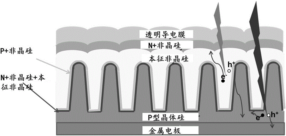
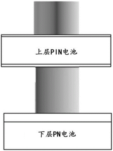
[0017] see figure 1 and figure 2 , a silicon nanowire-based thin-film silicon crystalline silicon laminated solar photovoltaic cell according to the present invention, the upper layer is a NIP amorphous silicon laminated cell, and the lower layer is a PIN heterojunction silicon cell. An array of silicon nanowires is located on the upper surface of the crystalline silicon of the absorber layer of the underlying cell. The silicon nanowire array plays the role of trapping light, which increases the travel of light in the amorphous silicon material, increases the absorption length, and reduces the actual thickness of the amorphous silicon layer, thereby suppressing the occurrence of light-induced attenuation.

[0018] The lower battery of the prese...


PUM


Abstract

The invention discloses a silicon nanowire-based thin-film silicon crystalline silicon laminated solar photovoltaic cell, which comprises an NIP amorphous silicon laminated cell located on an upper layer and a PIN heterojunction silicon cell located on a lower layer, wherein the NIP amorphous silicon laminated cell and the PIN heterojunction silicon cell are connected in series through an amorphous silicon tunnel junction; and a silicon nanowire array is arranged on the upper surface of crystalline silicon of an absorption layer of the PIN heterojunction silicon cell. The silicon nanowire array is introduced into the laminated cell, so that the cell has a light trapping advantage of the nanowire array, and relatively high open-circuit voltage and short-circuit current of the laminated cell at the same time.

Description

technical field [0001] The invention relates to the field of novel solar photovoltaic cell structures, in particular to a silicon nanowire-based thin-film silicon crystal silicon laminated solar photovoltaic cell. Background technique [0002] At present, most of the existing laminated battery technologies are laminated batteries based on thin film materials, and the research mainly focuses on multi-component compound laminated batteries, amorphous silicon laminated batteries and dye-sensitized laminated batteries. [0003] Amorphous silicon is a direct bandgap material with a high light absorption coefficient, and a 1-micron thick amorphous silicon film can absorb most of the energy in the visible light of sunlight. However, amorphous silicon materials have obvious light-induced attenuation effect, and the efficiency of photovoltaic cells is greatly attenuated. Using the laminated battery structure, the microcrystalline silicon battery is connected in series under the amor...

Claims


Application Information

Patent Timeline
Patent Type & Authority Applications(China)
IPC IPC(8): H01L31/076H01L31/077H01L31/028H01L31/0352
CPCH01L31/028H01L31/035227H01L31/076H01L31/077Y02E10/547Y02E10/548
Inventor 王珺郭群超朱红英丁云飞朱晨烜
Owner SHANGHAI DIANJI UNIV
Learn More