Preparation method of copper indium gallium diselenide film solar battery buffer layer
A technology of thin-film solar cells and copper indium gallium selenide, which is applied in the field of solar cells, can solve problems such as unfavorable, difficult to precisely control film layer growth, and damage to the absorbing layer, and achieve simple and easy process, saving production cost and space, and cost-effectiveness. The effect of dense and uniform film
- Summary
- Abstract
- Description
- Claims
- Application Information
AI Technical Summary
Problems solved by technology
Method used
Image

Examples
Embodiment 1
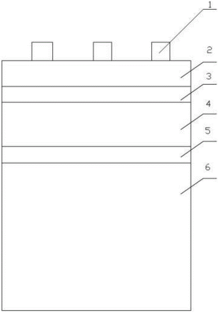
[0027] Glass is used as the copper indium gallium selenide thin-film solar cell substrate 6, and after the substrate 6 of the Mo bottom electrode 5 and the CIGS absorption layer 4 plated is placed in the reaction chamber of the atomic layer deposition equipment, the reaction chamber is evacuated to 0.5Pa, heating the substrate to 130℃, diethylzinc, H 2 S, H 2 O was used as the precursor source of Zn, S and O respectively, and ZnO thin film and ZnS thin film were alternately deposited 300 times each on the heated substrate by atomic layer deposition method. A ZnO thin film deposition is directed to the reaction chamber of the atomic layer deposition equipment, using high-purity nitrogen as a carrier gas to introduce diethyl zinc for 0.7s, then purging the reaction chamber with high-purity nitrogen for 3s, and then introducing water vapor for 0.3s to deposit A single layer of ZnO was obtained, and then the reaction chamber was purged with high-purity nitrogen for 3 s. A ZnS th...
Embodiment 2
[0029] Glass is used as the copper indium gallium selenide thin-film solar cell substrate 6, and after the substrate 6 of the Mo bottom electrode 5 and the CIGS absorption layer 4 plated is placed in the reaction chamber of the atomic layer deposition equipment, the reaction chamber is evacuated to 0.3Pa, heating the substrate to 150℃, diethylzinc, H 2 S, H 2 O was used as the precursor source of Zn, S, and O respectively, and ZnO thin film and ZnS thin film were alternately deposited 500 times each on the heated substrate by atomic layer deposition method. A ZnO thin film deposition is directed to the reaction chamber of the atomic layer deposition equipment, using high-purity nitrogen as a carrier gas to introduce diethyl zinc for 1 second, then purging the reaction chamber with high-purity nitrogen for 10 seconds, and then introducing water vapor for 0.7 seconds. single layer of ZnO, and then purged the reaction chamber with high-purity nitrogen for 10 s. A ZnS thin film ...
Embodiment 3
[0031] Glass is used as the copper indium gallium selenide thin-film solar cell substrate 6, and after the substrate 6 of the Mo bottom electrode 5 and the CIGS absorption layer 4 plated is placed in the reaction chamber of the atomic layer deposition equipment, the reaction chamber is evacuated to 0.4Pa, heating the substrate to 120℃, diethylzinc, H 2 S, H 2 O was used as the precursor source of Zn, S, and O respectively, and ZnO thin film and ZnS thin film were alternately deposited 400 times on the heated substrate by atomic layer deposition method. A ZnO thin film deposition is directed to the reaction chamber of the atomic layer deposition equipment, using high-purity nitrogen as a carrier gas to introduce diethyl zinc for 0.5s, then purging the reaction chamber with high-purity nitrogen for 6s, and then introducing water vapor for 1s to deposit single layer of ZnO, and then purging the reaction chamber with high-purity nitrogen for 6 s. A ZnS thin film deposition is to...
PUM
| Property | Measurement | Unit |
|---|---|---|
| thickness | aaaaa | aaaaa |
| thickness | aaaaa | aaaaa |
| thickness | aaaaa | aaaaa |
Abstract
Description
Claims
Application Information
 - R&D
- Intellectual Property
- Life Sciences
- Materials
- Tech Scout
- Unparalleled Data Quality
- Higher Quality Content
- 60% Fewer Hallucinations
Browse by: Latest US Patents, China's latest patents, Technical Efficacy Thesaurus, Application Domain, Technology Topic, Popular Technical Reports.
© 2025 PatSnap. All rights reserved.Legal|Privacy policy|Modern Slavery Act Transparency Statement|Sitemap|About US| Contact US: help@patsnap.com