ZnO-based nanorod/quantum well composite ultraviolet light-emitting diode and preparation method thereof
A technology of light-emitting diodes and nanorods, applied in semiconductor devices, electrical components, circuits, etc., can solve the problems of limiting the application of ZnO-based ultraviolet light emitters, low quantum efficiency of light-emitting diodes, poor interface quality, deep-level light emission, etc. Polarization effect, the effect of improving the quality of materials and interfaces, and improving the rate of radiation recombination
- Summary
- Abstract
- Description
- Claims
- Application Information
AI Technical Summary
Problems solved by technology
Method used
Image
Examples
Embodiment 1
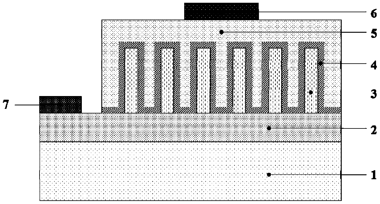
[0040] 1) Substrate cleaning: use sapphire as the substrate, cut it into a size of 15mm×15mm, ultrasonically clean it with acetone, alcohol and deionized water for 3 minutes, and finally use N 2 blow dry.
[0041] 2) Preparation of n-type ZnO thin film layer: Put the sapphire substrate after surface cleaning into the growth chamber of the radio frequency magnetron sputtering system, and the growth chamber is evacuated to the background pressure of 5×10 -4 Pa, heating the substrate to a temperature of 200°C. AZO ceramic target (ZnO:Al ceramic target) was selected as the target material for depositing n-type ZnO thin film layer. Before coating, pre-sputter for 10 min to remove impurities on the surface of the target, and then use radio frequency magnetron sputtering to deposit n-type ZnO thin film on the sapphire substrate. The temperature of the deposition substrate is 200° C., the gas during deposition is argon, the pressure is 0.5 Pa, the sputtering power is 60 W, and the s...
Embodiment 2
[0048] 1) Substrate cleaning: Use sapphire as the substrate, cut it into a size of 15mm×15mm, use acetone, alcohol, and deionized water to ultrasonically clean it for 3 minutes, and finally use N 2 blow dry.
[0049] 2) Preparation of n-type ZnO thin film layer: put the sapphire substrate after surface cleaning into the growth chamber of the radio frequency magnetron sputtering system, and vacuum the growth chamber to the background pressure of 1×10 -4 Pa, the substrate is heated to a temperature of 400 °C. AZO ceramic target is selected as the target material for depositing n-type ZnO thin film layer. Before coating, pre-sputter for 10 minutes to remove impurities on the surface of the target, and then use radio frequency magnetron sputtering to deposit an n-type ZnO thin film layer on the sapphire substrate; the temperature of the deposition substrate is 400 ° C, and the gas during deposition is Ar gas. The air pressure is 5.0Pa, the sputtering power is 150W, and the sputt...
Embodiment 3
[0056] 1) Substrate cleaning: Use sapphire as the substrate, cut it into a size of 15mm×15mm, use acetone, alcohol, and deionized water to ultrasonically clean it for 3 minutes, and finally use N 2 blow dry.
[0057] 2) Preparation of n-type ZnO thin film layer: put the sapphire substrate after surface cleaning into the growth chamber of the radio frequency magnetron sputtering system, and vacuum the growth chamber to the background pressure of 1×10 -3 Pa, heating the substrate to a temperature of 300°C. AZO ceramic target is selected as the target material for depositing n-type ZnO thin film layer. Before coating, pre-sputter for 10 min to remove impurities on the target surface. Then an n-type ZnO thin film layer was deposited on the sapphire substrate by radio frequency magnetron sputtering method. The temperature of the deposition substrate is 300° C., the gas during deposition is Ar gas, the gas pressure is 8.0 Pa, the sputtering power is 20 W, and the sputtering time ...
PUM
 Abstract
Description
Claims
Application Information
 - R&D
- Intellectual Property
- Life Sciences
- Materials
- Tech Scout
- Unparalleled Data Quality
- Higher Quality Content
- 60% Fewer Hallucinations
Browse by: Latest US Patents, China's latest patents, Technical Efficacy Thesaurus, Application Domain, Technology Topic, Popular Technical Reports.
© 2025 PatSnap. All rights reserved.Legal|Privacy policy|Modern Slavery Act Transparency Statement|Sitemap|About US| Contact US: help@patsnap.com


