
Method for producing silylene film through mechanical stripping, and application of silylene film

A mechanical peeling, silicene technology, applied in chemical instruments and methods, inorganic chemistry, silicon compounds, etc., can solve problems such as being unsuitable for large-scale industrial production, high cost of silicene, increasing metal films and substrate materials, etc. Environmental friendliness, less environmental pollution, and the effect of reducing production costs

Active Publication Date: 2017-04-05
日照东润有机硅股份有限公司
View PDF6 Cites 5 Cited by
  • Summary
  • Abstract
  • Description
  • Claims
  • Application Information

AI Technical Summary

Problems solved by technology

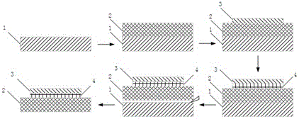
[0008] Aiming at the technical problem that the cost of preparing silicene by physical and chemical vapor deposition is very high and it is not suitable for large-scale industrial production, the present invention proposes a silicene film prepared by mechanical exfoliation and the application of the obtained silicene film in batteries. The two-dimensional nanomaterial physically covers the passivated silicon surface of the metal film. After the temperature change treatment, the sample is dispersed in a solvent liquid with a surfactant, and the friction between the metal film and the base material is increased by ultrasonic stirring, and the two-dimensional nanomaterial and the Silicene exfoliated from silicon substrates to obtain silicene films

Method used


Image

  • Method for producing silylene film through mechanical stripping, and application of silylene film
  • Method for producing silylene film through mechanical stripping, and application of silylene film

Examples


Embodiment 1

[0042] Such as figure 1 As shown, the method steps of the silicene film prepared by mechanical peeling in the present invention are as follows:

[0043] (1) Select a Si (111) silicon wafer with a diameter of 50 mm and a thickness of 0.1 mm as the silicon source, wash it with SPM solution at a temperature of 80 °C for 5 minutes, rinse it with deionized water, and then ultrasonicate it in HF solution for 1 Minutes to remove the silicon oxide on the surface of the silicon wafer, and finally rinse with deionized water to remove the residual HF liquid, and dry the surface of the silicon wafer with hot nitrogen. Among them, the SPM solution is H 2 SO 4 :H 2 o 2 =1:4 strong oxidizing solution, the concentration of HF solution is 3.5%, the hot nitrogen is nitrogen with a purity of 99.9%, and the temperature is 80°C.

[0044] (2) Take out the processed Si wafer and put it into a vacuum chamber. The temperature of the Si wafer is at room temperature, and the background vacuum degre...

Embodiment 2

[0050] (1) Select a Si (111) silicon wafer with a diameter of 70 mm and a thickness of 0.2 mm as the silicon source, wash it with SPM solution at a temperature of 80 °C for 5 minutes, rinse it with deionized water, and then ultrasonicate it in HF solution for 1 Minutes to remove the silicon oxide on the surface of the silicon wafer, and finally rinse with deionized water to remove the residual HF liquid, and dry the surface of the silicon wafer with hot nitrogen. Among them, the SPM solution is H 2 SO 4 :H 2 o 2 =1:4.5 strong oxidizing solution, the concentration of HF solution is 4%, the hot nitrogen is nitrogen with a purity of 99.9%, and the temperature is 85°C.

[0051] (2) Take out the processed Si wafer and put it into a vacuum chamber. The temperature of the Si wafer is at room temperature, and the background vacuum degree of the coating is 1.0×10 -3 Pa, using resistance wire evaporation, using a crystal oscillator to monitor the coating process, setting the evapora...

Embodiment 3

[0057] (1) Select a Si (111) silicon wafer with a diameter of 80 mm and a thickness of 0.25 mm as the silicon source, wash it with SPM solution at a temperature of 80 °C for 5 minutes, rinse it with deionized water, and then ultrasonicate it in HF solution for 1 Minutes to remove the silicon oxide on the surface of the silicon wafer, and finally rinse with deionized water to remove the residual HF liquid, and dry the surface of the silicon wafer with hot nitrogen. Among them, the SPM solution is H 2 SO 4 :H 2 o 2 =1:5 strong oxidizing solution, the concentration of HF solution is 4.5%, the hot nitrogen is nitrogen with a purity of 99.9%, and the temperature is 85°C.

[0058] (2) Take out the processed Si wafer and put it into a vacuum chamber. The temperature of the Si wafer is at room temperature, and the background vacuum degree of the coating is 1.0×10 -3 Pa, using sputtering method for coating, using Mo metal target, using a crystal oscillator to monitor the coating pr...


PUM

PropertyMeasurementUnit
Thicknessaaaaaaaaaa
Thicknessaaaaaaaaaa
Thicknessaaaaaaaaaa

Abstract

The invention discloses a silylene film produced through mechanical stripping, and an application of the obtained silylene film in batteries. A production method of the silylene film comprises the following steps: physically covering the silicon surface of a metal film with a two-dimensional nanomaterial, carrying out high temperature treatment to diffuse the silicon element to the interface of the two-dimensional nanomaterial and the metal film, decreasing the temperature to room temperature, dispersing a sample in a surfactant-containing solvent liquid, allowing polar molecules to easily enter the interface of the metal film and the above substrate material, carrying out ultrasonic stirring to increase friction of the metal film and the substrate material, and stripping the two-dimensional nanomaterial and silylene from the silicon substrate to obtain the silylene film. The silylene film is mechanically stripped from a liquid phase under the physical action, so physical properties of a silylene material are protected, high vacuum and high danger gas working environment is avoided, and use of severely toxic organic reactants is avoided; and the two-dimensional nanomaterial can be used repeatedly, so the cost is reduced, and the silylene film has wide market application values in the field of solar batteries.

Description

technical field [0001] The invention relates to the field of nanomaterial preparation, in particular to a method for preparing silicene by mechanical exfoliation and the application of the obtained silicene in batteries. Background technique [0002] Silicon and carbon belong to Group IV elements of the periodic table of elements, and also occupy an extremely important position in nature and materials science. In 2007, Verri et al. proposed that silicon can form a single atomic layer structure similar to graphite and named it silicene. A series of subsequent theoretical work showed that silicene has a Dirac-type electronic structure similar to graphene, and its Brillouin zone also has six linearly dispersed Dirac cones. As a result, most novel quantum effects found in graphene have corresponding versions in silicene. Moreover, the silicene system also has some advantages that the graphene system does not have. For example, silicene has stronger spin-orbit coupling, so it c...

Claims


Application Information

Patent Timeline
IPC IPC(8): C01B33/021H01L51/44B82Y30/00
CPCB82Y30/00C01B33/021H10K30/81Y02E10/549
Inventor 陈庆曾军堂王镭迪
Owner 日照东润有机硅股份有限公司
Learn More