Thin film transistor, manufacturing method thereof, display substrate and display device

A technology for thin film transistors and fabrication methods, applied in transistors, semiconductor/solid-state device manufacturing, semiconductor devices, etc., can solve the problems of unstable threshold voltage, unfavorable application, increased cost and process complexity, etc., and achieves improved uniformity, improved Stable, low-cost effect

Active Publication Date: 2018-09-14
BOE TECH GRP CO LTD
View PDF5 Cites 0 Cited by
  • Summary
  • Abstract
  • Description
  • Claims
  • Application Information

AI Technical Summary

Problems solved by technology

[0004] In the existing low-temperature polysilicon thin film, due to the existence of a large number of grain boundary defect states, the threshold voltage of the thin film transistor is unstable and the carrier mobility is not good, and when the size of the thin film transistor shrinks, the problem of unstable threshold voltage will become more serious
Currently, ELA (excimer laser annealing) and CW solid-state laser two-step processing methods are generally used to improve the uniformity of low-temperature polysilicon films, but this increases the cost and complexity of the process, which is not conducive to practical applications.

Method used


Image

  • Thin film transistor, manufacturing method thereof, display substrate and display device
  • Thin film transistor, manufacturing method thereof, display substrate and display device
  • Thin film transistor, manufacturing method thereof, display substrate and display device

Examples


Embodiment 1

[0049] This embodiment provides a method for manufacturing a thin film transistor, the thin film transistor includes a gate, a source, a drain and an active layer, and the step of forming the active layer includes:

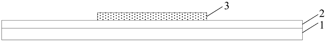
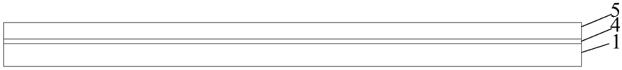
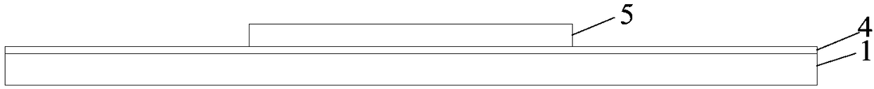
[0050] Form the graphics of the insulation layer;

[0051] Forming a pattern of an amorphous silicon layer on the heat insulating layer, the pattern of the amorphous silicon layer including a first part located on the heat insulating layer and a second part beyond the heat insulating layer;

[0052] The pattern of the amorphous silicon layer is processed by laser annealing process to form the active layer composed of polysilicon.

[0053]In this embodiment, the pattern of the amorphous silicon layer includes a first part located on the thermal insulation layer and a second part beyond the thermal insulation layer. After the amorphous silicon layer is laser annealed, the second part beyond the thermal insulation layer is cooled It will nucleate first if it is fast...

Embodiment 2

[0089] This embodiment provides a kind of thin film transistor, which is manufactured by adopting the above-mentioned manufacturing method. The thin film transistor includes an active layer composed of polysilicon located on the heat insulating layer, and the active layer includes a part located on the heat insulating layer. And the part beyond the insulation layer.

[0090] Since the pattern of the amorphous silicon layer is formed on the thermal insulation layer during the formation of the active layer of the thin film transistor, the pattern of the amorphous silicon layer includes a first part located on the thermal insulation layer and a portion beyond the thermal insulation layer. The second part outside of the thermal insulation layer is processed by laser annealing process on the pattern of the amorphous silicon layer. After the laser annealing of the amorphous silicon layer, the second part beyond the thermal insulation layer is cooled faster and will first nucleate , ...

Embodiment 3

[0092] This embodiment provides a display substrate, including the above-mentioned thin film transistor. Since the carrier mobility of the thin film transistor is relatively high and the threshold voltage is relatively stable, compared with the existing display substrate, the performance of the display substrate of this embodiment will be more reliable.


PUM


Abstract

The invention provides a thin film transistor, a manufacturing method thereof, a display substrate and a display device, and belongs to the field of display technology. The thin film transistor includes a gate, a source, a drain and an active layer, and the step of forming the active layer includes: forming a pattern of an insulating layer; forming a pattern of an amorphous silicon layer on the insulating layer, the The pattern of the amorphous silicon layer includes a first part located on the thermal insulation layer and a second part beyond the thermal insulation layer; the pattern of the amorphous silicon layer is processed by a laser annealing process so that the amorphous silicon A layer grows grains in a direction from said second portion to said first portion, forming said active layer composed of polysilicon. The technical solution of the present invention can prepare a polysilicon active layer with larger grain size and better uniformity at a lower cost, thereby improving the carrier mobility and the stability of the threshold voltage of the thin film transistor.

Description

technical field [0001] The present invention relates to the field of display technology, in particular to a thin film transistor, a manufacturing method thereof, a display substrate and a display device. Background technique [0002] Active Matrix Organic Light Emitting Diode (AMOLED) has the advantages of low energy consumption, low production cost, wide viewing angle, and fast response speed, so AMOLED has gradually replaced traditional liquid crystal displays. [0003] At present, AMOLED drives the organic light-emitting layer to emit light through a drive transistor (Drive Thin Film Transistor, DTFT). In order to make the DTFT have a higher carrier mobility, low-temperature polysilicon is generally used to make the active layer of the DTFT. [0004] In the existing low-temperature polysilicon thin film, due to the existence of a large number of grain boundary defect states, the threshold voltage of the thin film transistor is unstable and the carrier mobility is not good...

Claims


Application Information

Patent Timeline
Patent Type & Authority Patents(China)
IPC IPC(8): H01L21/77H01L29/786H01L27/12
CPCH01L27/1222H01L27/1281H01L29/78675H01L29/66757H01L27/1285H10K59/1213H10K50/87
Inventor 李小龙李栋张慧娟刘政
Owner BOE TECH GRP CO LTD
Why Eureka
Try Eureka