Polysilicon preparation apparatus and method

A polysilicon preparation and amorphous silicon layer technology, which is applied in the growth of polycrystalline materials, chemical instruments and methods, and crystal growth, can solve the problems affecting the electron mobility of polysilicon, small grains, and many grain boundaries between grains. Achieve the effect of increasing electron mobility and increasing size

Active Publication Date: 2015-11-25
SHENZHEN CHINA STAR OPTOELECTRONICS TECH CO LTD
View PDF9 Cites 0 Cited by
  • Summary
  • Abstract
  • Description
  • Claims
  • Application Information

AI Technical Summary

Problems solved by technology

During recrystallization, it will crystallize from low energy to high energy, and from low temperature to high temperature; so the starting point and direction of crystallization are messy, such as figure 2 As shown; resulting in smaller grains after crystallization and more grain boundaries between grains, thus affecting the electron mobility of polysilicon

Method used


Image

  • Polysilicon preparation apparatus and method
  • Polysilicon preparation apparatus and method
  • Polysilicon preparation apparatus and method

Examples


Embodiment Construction

[0031] The word "embodiment" used in this specification means serving as an example, example, or illustration. In addition, the article "a" used in this specification and the appended claims can generally be interpreted as meaning "one or more" unless specified otherwise or clearly directed to the singular form from the context.

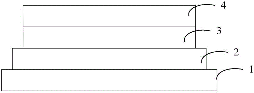
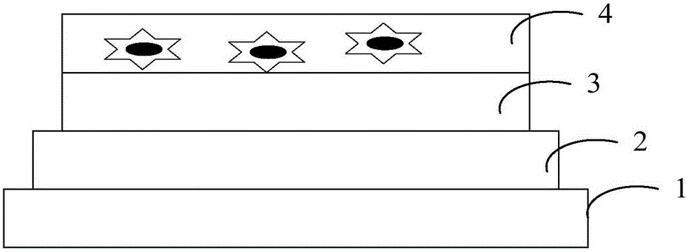
[0032] In the present invention, a plurality of mirrors and a diffuse reflection layer are provided on the surface of the support platform. The diffuse reflection layer is provided between the mirror and the mirror, and when laser annealing is performed, the diffuse reflection layer penetrates the non When the laser of the crystalline silicon layer is irradiated on the diffuse reflection layer area, diffuse reflection occurs; when irradiated on the mirror area, the reflected laser energy is concentrated on the amorphous silicon layer, so that the amorphous silicon in the area can be It absorbs energy and forms an energy gradient with other areas. There...


PUM


Abstract

A disclosed polysilicon preparation apparatus comprises a supporting platform, the surface of the supporting platform is provided with a reflection layer which possesses multiple reflection mirrors and a diffuse reflection layer; and the diffuse reflection layer is arranged among the reflection mirrors; the reflection layer is provided with a glass base plate, the glass base plate is provided with a buffer layer, and the buffer layer is provided with an amorphous silicon layer. When laser annealing is performed, diffuse reflection is generated when laser penetrating the amorphous silicon layer irradiates the diffuse reflection layer, reflected laser is gathered on the amorphous silicon layer when the reflection mirrors are irradiated, so that amorphous silicon at the area is capable of absorbing energy and energy gradient is formed on the area and the other area. According to the apparatus and the method, the crystallization direction can be controlled, the growth direction of polysilicon is controlled, the size of the crystal particle is raised, and the electron migration rate of polysilicon is improved.

Description

【Technical Field】 [0001] The invention relates to the field of display technology, in particular to a polysilicon preparation device and method. 【Background technique】 [0002] With the development of flat panel displays, the demand for high-resolution, low-energy panels is constantly being proposed. Amorphous silicon has low electron mobility. Low-temperature polysilicon can be produced at low temperatures and has high electron mobility, and it can be made C- MOS circuits are therefore widely studied to meet the requirements of high resolution and low energy consumption of panels. [0003] Current methods for making low-temperature polysilicon include solid phase crystallization (SPC), metal induced crystallization (MIC) and excimer laser annealing (ELA), among which excimer laser annealing is currently the most widely used method. [0004] Such as figure 1 As shown; the polysilicon preparation device includes: a support platform 1, a glass substrate 2 is provided on the surface of...

Claims


Application Information

Patent Timeline
Patent Type & Authority Applications(China)
IPC IPC(8): C30B28/02C30B29/06C30B30/00
Inventor 余威
Owner SHENZHEN CHINA STAR OPTOELECTRONICS TECH CO LTD
Why Eureka
Try Eureka