Solder resist composition, and coated printed wiring board
A technology for printed wiring boards and compositions, applied in the field of solder resist compositions and coated printed wiring boards, capable of solving problems such as resolution reduction
- Summary
- Abstract
- Description
- Claims
- Application Information
AI Technical Summary
Problems solved by technology
Method used
Image
Examples
Embodiment 1~5、 comparative example 1~3
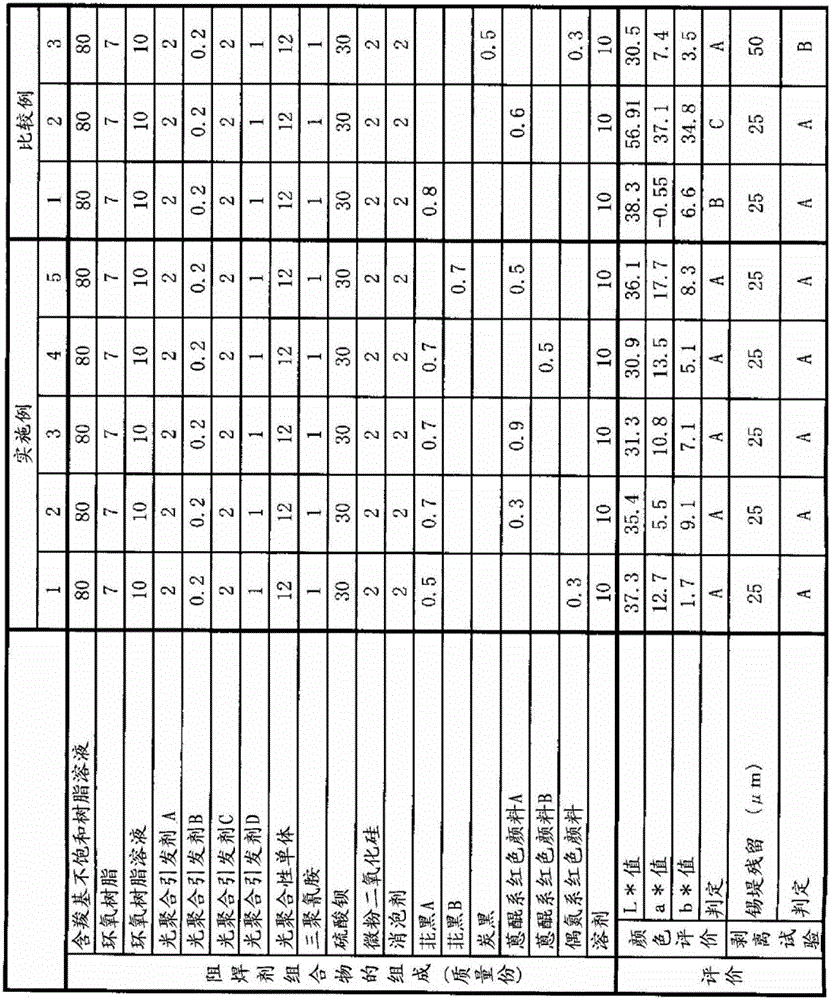
[0229] These components were mixed in the ratio shown in Table 1, thereby preparing a solder resist composition.
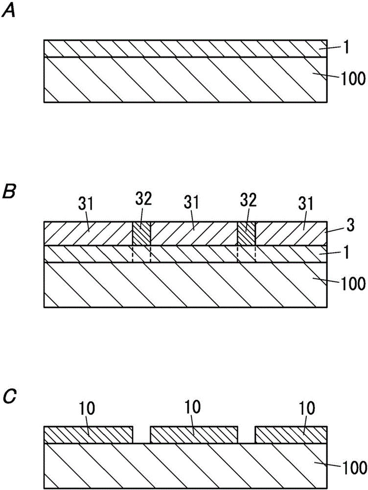
[0230] In addition, a wiring board provided with copper conductor wiring with a line width / line pitch of 0.2 mm / 0.3 mm and a thickness of 35 μm was prepared. The solder resist composition is applied on the surface of the wiring board by a screen printing method to form a wet coating film. The wet coating film was heated at 80°C for 20 minutes to perform preliminary drying to form a dry coating film having a thickness of 20 μm.
[0231] A mask for forming tin banks with widths of 25 μm, 50 μm, 75 μm, and 100 μm is closely attached to the dried coating film, and the irradiation energy density is 400 mJ / cm 2 Under the condition of irradiating ultraviolet rays, the dry coating film on the wiring substrate is selectively exposed.
[0232] The exposed dry coating film is subjected to a development process with a sodium carbonate aqueous solution, so that the part cured by the...
Embodiment 6~10、 comparative example 4~6
[0263] These components were mixed in the ratio shown in Table 2 below, thereby preparing a second resist composition.
[0264] [Table 2]
[0265] Raw material of the second resist composition Composition (parts by mass) Unsaturated resin solution containing carboxyl group80 Photopolymerizable monomer12 Crystalline epoxy compound20 Photopolymerization initiator A6 Photopolymerization initiator B0.15 Barium sulfate50 Micronized silica3.5 Melamine0.6 Green colorant1.1 Defoamer3 Solvent 7
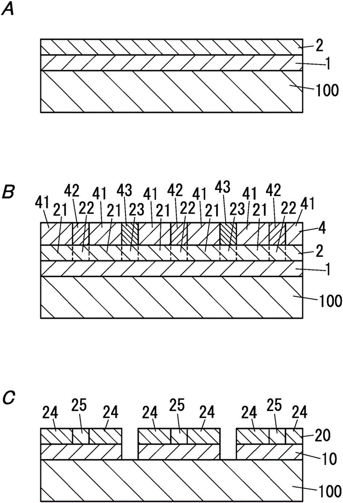
[0266] In addition, a wiring board provided with copper conductor wiring with a line width / line pitch of 0.2 mm / 0.3 mm and a thickness of 35 μm was prepared. The solder resist composition used in Examples 1 to 5 and Comparative Examples 1 to 3 was coated on the surface of the wiring board by a screen printing method, thereby forming a first coating film. The first coating film was pre-dried by heating at 80°C for 20 minutes, and the thickness was 20 μm.
[0267] The second resist comp...
PUM
| Property | Measurement | Unit |
|---|---|---|
| acid value | aaaaa | aaaaa |
| acid value | aaaaa | aaaaa |
| acid value | aaaaa | aaaaa |
Abstract
Description
Claims
Application Information
 - R&D
- Intellectual Property
- Life Sciences
- Materials
- Tech Scout
- Unparalleled Data Quality
- Higher Quality Content
- 60% Fewer Hallucinations
Browse by: Latest US Patents, China's latest patents, Technical Efficacy Thesaurus, Application Domain, Technology Topic, Popular Technical Reports.
© 2025 PatSnap. All rights reserved.Legal|Privacy policy|Modern Slavery Act Transparency Statement|Sitemap|About US| Contact US: help@patsnap.com


