Solar cell and method for manufacturing solar cell

一种太阳能电池、电极的技术,应用在半导体/固态器件制造、电路、光伏发电等方向,能够解决填充因数降低、配线电阻大等问题

Active Publication Date: 2017-02-22
SHIN ETSU CHEM CO LTD
View PDF3 Cites 8 Cited by
  • Summary
  • Abstract
  • Description
  • Claims
  • Application Information

AI Technical Summary

Problems solved by technology

However, in the solar cell of Patent Document 1, the bus-bar electrodes (N-type bus-bar electrodes 22, P-type bus-bar electrodes 23) are only formed in pairs on the outer periphery of the substrate (refer to Figure 16 )
In the case of this configuration, since the length of the electrode fingers is long, the wiring resistance is very large, resulting in a decrease in the fill factor

Method used


Image

  • Solar cell and method for manufacturing solar cell
  • Solar cell and method for manufacturing solar cell
  • Solar cell and method for manufacturing solar cell

Examples


Embodiment 1~4

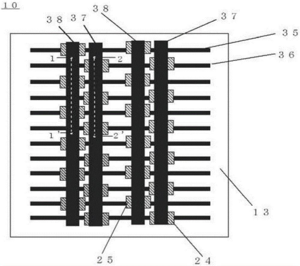
[0170] In Examples 1 to 4, the formation of Figure 7 The electrode part, insulating film, electrode line part and electrode bus bar part ( Figure 6 j~l).

[0171] First, the electrode portion was formed in a linear pattern with a width of 100 μm. Specifically, using screen printing, a conductive paste (sintering paste) composed of silver (Ag) particles, glass paste, binder, and solvent is coated on a specific position on the diffusion layer, dried, and dried at 700 ℃ for 5 minutes to form the first electrode part and the second electrode part. Next, an insulating film having a length of 3 mm and a width of 500 μm was formed in the insulating region. Polyimide paste was used as the material of the insulating film, and this paste was applied to a specific part by screen printing, and it was cured by heating at 150° C. for 20 minutes to form an insulating film.

[0172] Next, finger electrodes (electrode line portions) having a width of 100 μm and bus bar electrodes (electr...

Embodiment 5~8

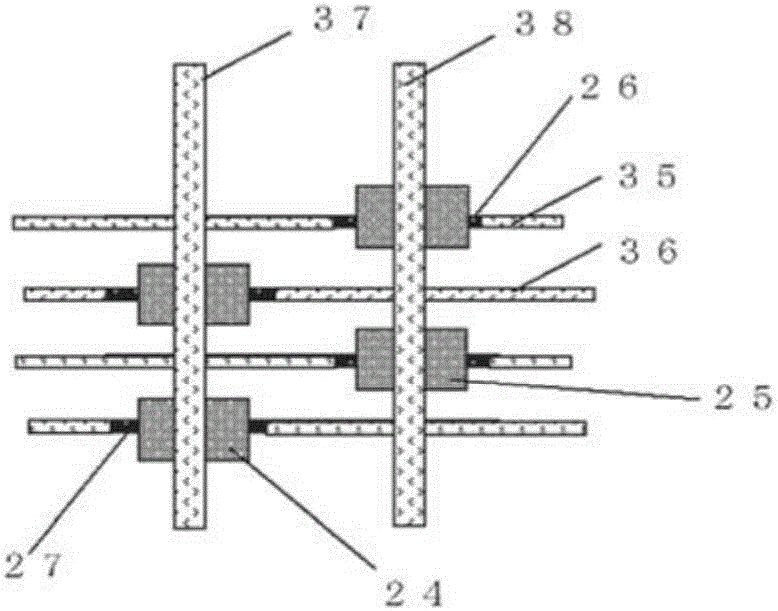
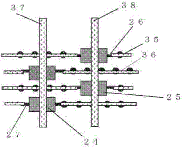
[0175] In embodiment 5~8, form such as Figure 8 The electrode part, insulating film, electrode line part and electrode bus bar part ( Figure 6 j~l).

[0176] formed as Figure 8 The electrode part of the pattern shown. Patterns having a diameter of 200 μm were provided at intervals of 0.5 mm along the extending direction of the diffusion layer, except for the portion where the insulating film was formed. In addition, only the insulating region is a linear pattern with a length of 4 mm and a width of 100 μm. The sintering paste was applied by screen printing, dried, and calcined at 700° C. for 5 minutes to form this pattern. Next, an insulating film having a length of 3 mm and a width of 500 μm was formed in the insulating region. Polyimide paste was used as the material of the insulating film, and the paste was applied to a specific position by screen printing, and was cured by heating at 150° C. for 20 minutes to form an insulating film.

[0177] Next, an electrode li...


PUM


Abstract

The present invention is a solar cell wherein: a diffusion layer of a first conductivity type and a diffusion layer of a second conductivity type are formed on a surface of a substrate, said surface being on the reverse side of a light-receiving surface of the substrate; a first electrode part, a second electrode part, a first electrode line part, a second electrode line part, a first electrode bus bar part and a second electrode bus bar part are arranged; a first insulating film is formed so as to cover the lateral surface part and the upper part of the second electrode part in a region where the second electrode part and the first electrode bus bar part intersect with each other; a second insulating film is formed so as to cover the lateral surface part and the upper part of the first electrode part in a region where the first electrode part and the second electrode bus bar part intersect with each other; the second electrode part is continuously formed in the form of a line immediately below the first insulating film; and the first electrode part is continuously formed in the form of a line immediately below the second insulating film. Consequently, the present invention provides: a back contact solar cell which has low wiring resistance and high conversion efficiency; and a method for manufacturing a solar cell, which is capable of manufacturing such a back contact solar cell at low cost.

Description

technical field [0001] The invention relates to a solar cell and a method for manufacturing the solar cell. Background technique [0002] Figure 15 It is a cross-sectional view schematically showing a conventional back electrode type solar cell. refer to Figure 15 , the back electrode type solar cell 110 produced using conventional techniques will be described. A concavo-convex shape 114 is formed on the light-receiving surface side of the N-type silicon substrate 113 , and an N-type diffusion layer, that is, a Front Surface Field (FSF) layer 115 is formed. Further, a dielectric passivation layer (surface passivation layer) 117 containing silicon dioxide and an antireflection film 116 containing silicon nitride are formed on the concave-convex shape 114 from the side of the N-type silicon substrate 113 . [0003] Furthermore, an oxide layer (first rear passivation film) 119 is formed on the back surface of the N-type silicon substrate 113 . Further, N-type doped N-type ...

Claims


Application Information

Patent Timeline
Patent Type & Authority Applications(China)
IPC IPC(8): H01L31/0224H01L21/28H01L31/068
CPCY02E10/547H01L31/022441H01L31/022433H01L31/0682H01L21/28H01L31/02002H01L31/0224H01L31/02366H01L31/068Y02E10/50H01L31/0201H01L31/02167H01L31/022458
Inventor 远洞阳子渡部武纪大塚宽之
Owner SHIN ETSU CHEM CO LTD
Why Eureka
Try Eureka