
Method for manufacturing silicon carbide semiconductor device

A manufacturing method and technology of silicon carbide, applied in semiconductor/solid-state device manufacturing, semiconductor devices, electrical components, etc., can solve problems such as increased leakage current, and achieve the effect of good yield

Active Publication Date: 2019-10-11
FUJI ELECTRIC CO LTD
View PDF9 Cites 0 Cited by
  • Summary
  • Abstract
  • Description
  • Claims
  • Application Information

AI Technical Summary

Problems solved by technology

[0020] However, in the technologies described in the above-mentioned Patent Documents 1 to 8, there arises a problem that, in the above-mentioned Patent Document 1, the remaining of defects introduced into the semiconductor substrate by proton injection (carrier (electron / hole) mobility ) is described, but there is a problem of poor characteristics such as an increase in leakage current due to the existence of a crystal defect layer near the back surface of the substrate.

Method used


Image

  • Method for manufacturing silicon carbide semiconductor device
  • Method for manufacturing silicon carbide semiconductor device
  • Method for manufacturing silicon carbide semiconductor device

Examples


Embodiment approach 1

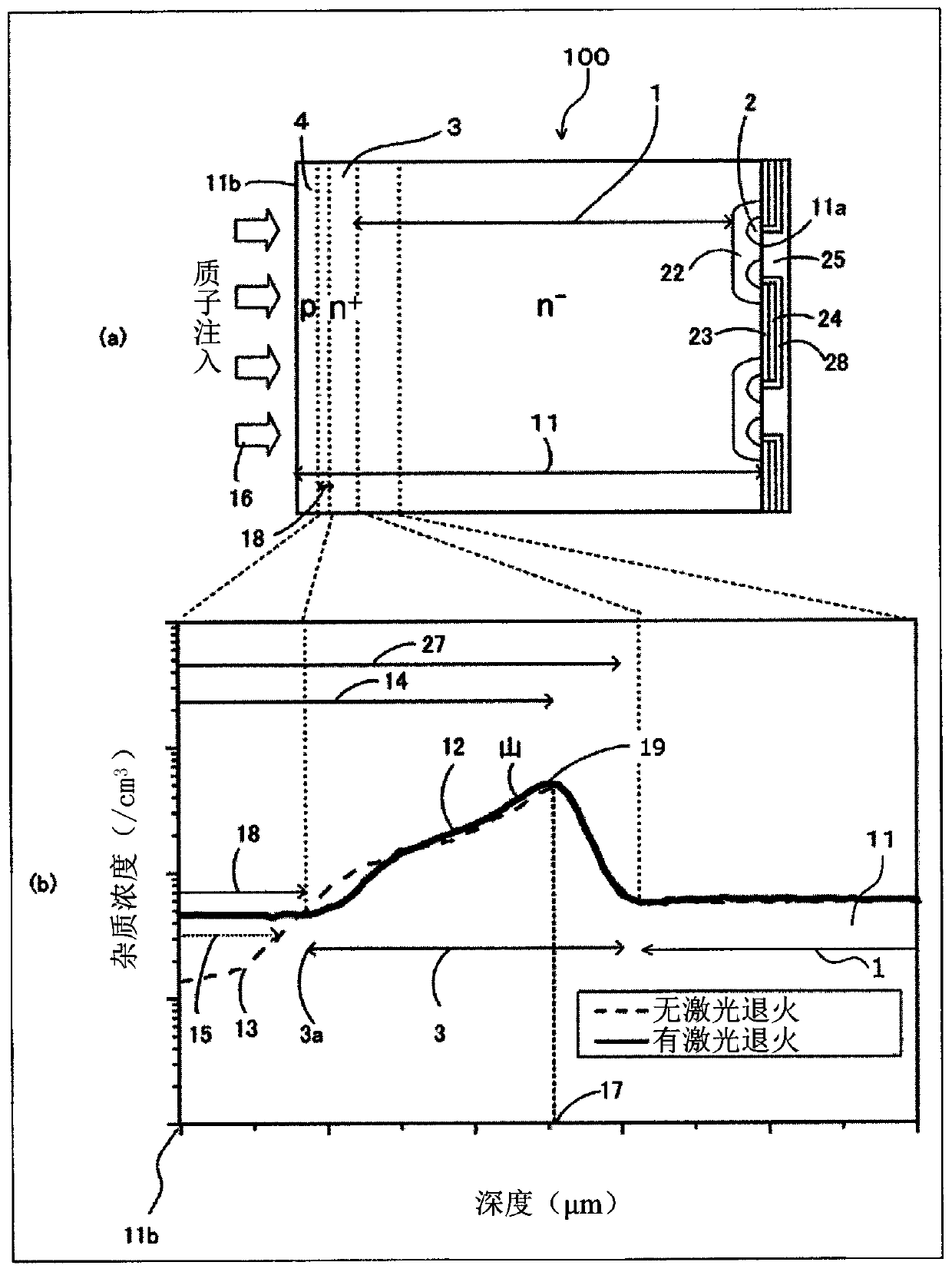
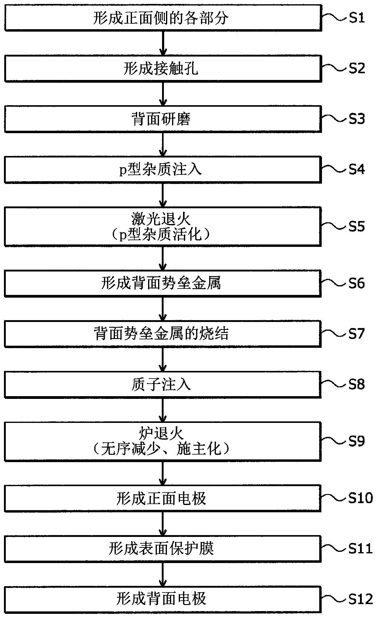
[0080] As an example of a silicon carbide semiconductor device fabricated by the method of manufacturing a silicon carbide (SiC) semiconductor device according to Embodiment 1, a structure of a planar gate type IGBT (hereinafter referred to as SiC-IGBT) will be described. figure 1 It is an explanatory diagram showing the structure of a semiconductor device manufactured by the method of manufacturing a silicon carbide semiconductor device according to the first embodiment. figure 1 (a) shows a cross-sectional view of main parts of SiC-IGBT 100, figure 1 (b) shows n + The doping concentration curve near the type field stop layer 3. Such as figure 1 As shown, the silicon carbide semiconductor device of Embodiment 1 becomes n - type drift layer 1 n - The front side 11a side of the silicon carbide substrate (semiconductor chip) 11 is provided with a p-type base (base) region 22, n + A MOS gate structure composed of a type emitter region 2, a gate insulating film 23 and a gate ...

Embodiment approach 2

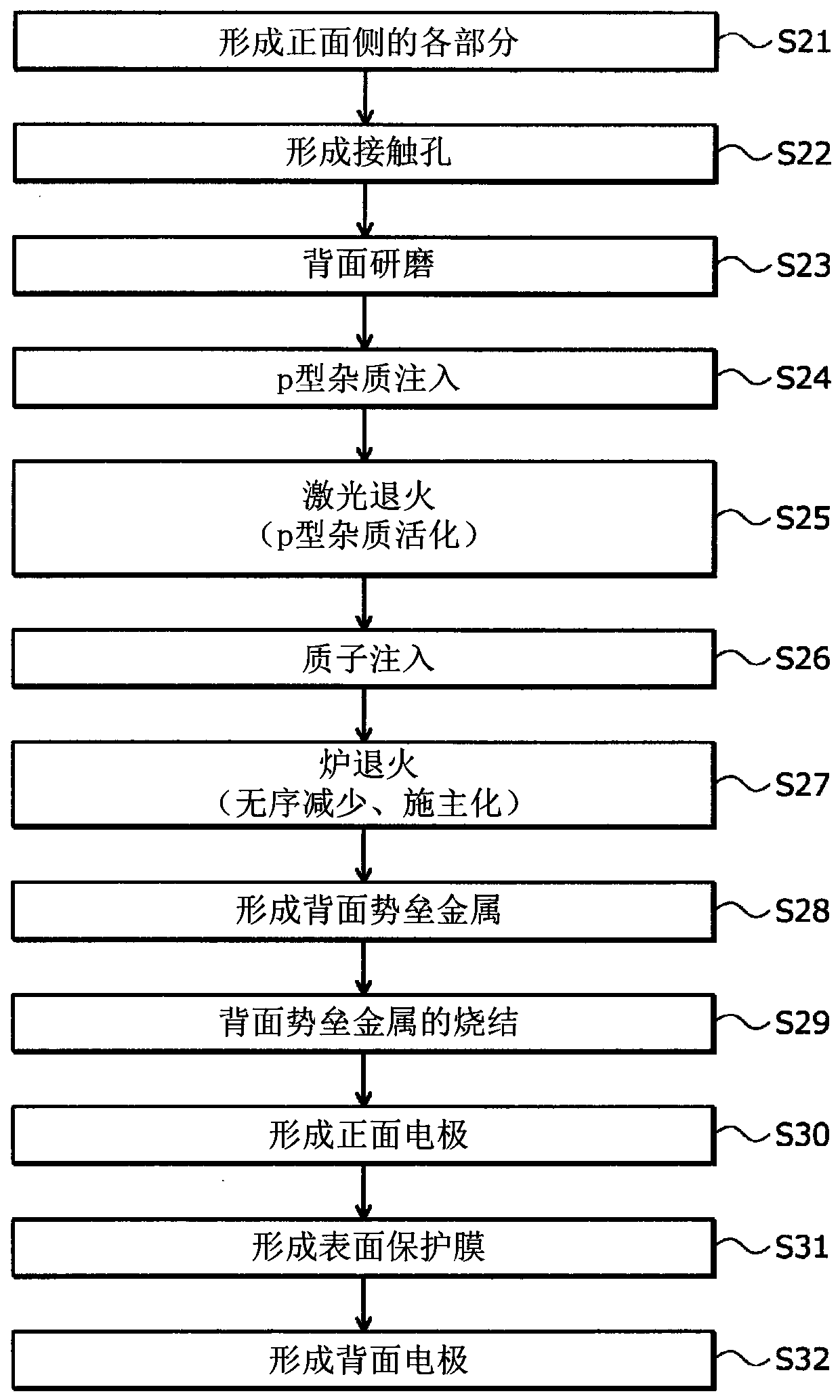
[0105] Next, a method of manufacturing a silicon carbide semiconductor device according to Embodiment 2 will be described. Figure 3A It is a flowchart showing the outline of a method of manufacturing a silicon carbide semiconductor device according to the second embodiment. The difference between the method of manufacturing a silicon carbide semiconductor device in Embodiment 2 and the method of manufacturing a silicon carbide semiconductor device in Embodiment 1 is that the formation of the back barrier metal and the sintering of the back barrier metal are combined with proton injection 16 and furnace annealed for a replacement pair.

[0106] Specifically, after the steps from formation of each part on the front side to laser annealing (steps S21 to S25) are sequentially performed in the same manner as in the first embodiment, proton implantation 16, furnace annealing, back barrier metal The steps of forming and sintering the back barrier metal (steps S26 to S29). The meth...

Embodiment approach 3

[0109] Next, a method of manufacturing a silicon carbide semiconductor device according to Embodiment 3 will be described. Figure 3B It is a flowchart showing the outline of a method of manufacturing a silicon carbide semiconductor device according to the third embodiment. The difference between the manufacturing method of the silicon carbide semiconductor device in the third embodiment and the manufacturing method of the silicon carbide semiconductor device in the second embodiment is that the laser annealing is performed after the proton implantation 16 and before the formation of the back barrier metal.

[0110] Specifically, steps from formation of each portion on the front side to ion implantation of p-type impurities are sequentially performed in the same manner as in the first embodiment (steps S41 to S44 ). Next, proton injection 16 is performed (step S45). The method and condition of proton implantation 16 and step S8 of embodiment one (referring to figure 2 )same...


PUM


Abstract

After the front component structure is formed, from n ‑ P-type impurities are ion-implanted into the back surface (11b) of the silicon carbide substrate (11). Next, from n ‑ The back surface (11b) of the silicon carbide substrate (11) is irradiated with laser light to activate the p-type impurities to form a p-type collector layer (4). Next, in n ‑ A barrier metal layer is formed on the back surface (11b) of the silicon carbide substrate (11), and the barrier metal layer is sintered. Next, from n ‑ Proton implantation (16) with a range (17) at a position deeper than the p-type collector layer (4) is performed on the back surface (11b) side of the type silicon carbide substrate (11). Next, n is subjected to furnace annealing ‑ The entire silicon carbide substrate (11) is heated to convert protons into donors to form n-type silicon carbide substrates (11). + type field cutoff layer (3). At this time, n is reduced by reducing the disorder remaining in the proton passage region (14). ‑ Crystal state recovery of type silicon carbide substrate (11). This makes it possible to stably avoid electrical characteristic defects.

Description

technical field [0001] The invention relates to a method for manufacturing a silicon carbide semiconductor device. Background technique [0002] Examples of power semiconductor devices include semiconductor devices such as diodes made of silicon (Si) and IGBTs (Insulated Gate Bipolar Transistor: Insulated Gate Bipolar Transistor) having a withstand voltage of 400V, 600V, 1200V, 1700, 3300V or higher. These semiconductor devices are used in power conversion devices such as converters and inverters. Such power semiconductor devices are required to have good electrical characteristics such as low loss, high efficiency, and high breakdown resistance, and low cost. [0003] The following method has been proposed as a method of manufacturing the semiconductor device for electric power. First, after becoming n - type drift layer n - On the front side of the type semiconductor substrate, a front element structure such as a diffusion region and / or a MOS gate (insulated gate compos...

Claims


Application Information

Patent Timeline
Patent Type & Authority Patents(China)
IPC IPC(8): H01L29/739H01L21/265H01L21/329H01L21/336H01L29/12H01L29/78H01L29/861H01L29/868
CPCH01L21/265H01L29/78H01L29/868H01L29/66068H01L21/046H01L21/268H01L29/6606H01L29/1608H01L29/32H01L29/36H01L29/7397H01L29/861H01L21/02529H01L21/02609H01L21/02694H01L21/26506H01L21/324H01L29/0615H01L29/66348
Inventor 栗林秀直宫崎正行
Owner FUJI ELECTRIC CO LTD
Learn More