Fabrication of semi-polar crystal structures

A technology of crystal structure and anisotropy, applied in semiconductor/solid-state device manufacturing, semiconductor devices, electrical components, etc., can solve problems such as difficulties

Inactive Publication Date: 2017-02-22
SEREN PHOTONICS
View PDF3 Cites 2 Cited by
  • Summary
  • Abstract
  • Description
  • Claims
  • Application Information

AI Technical Summary

Problems solved by technology

It has proven very difficult

Method used


Image

  • Fabrication of semi-polar crystal structures
  • Fabrication of semi-polar crystal structures
  • Fabrication of semi-polar crystal structures

Examples


Embodiment Construction

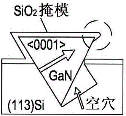
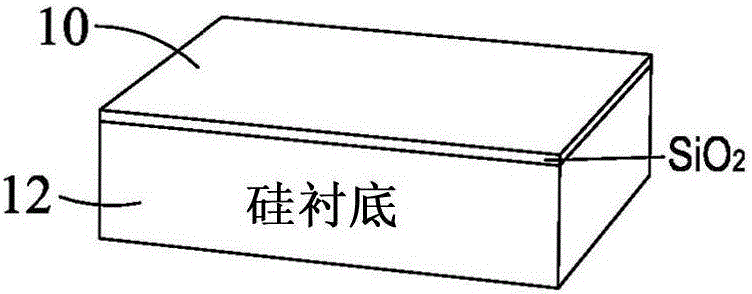
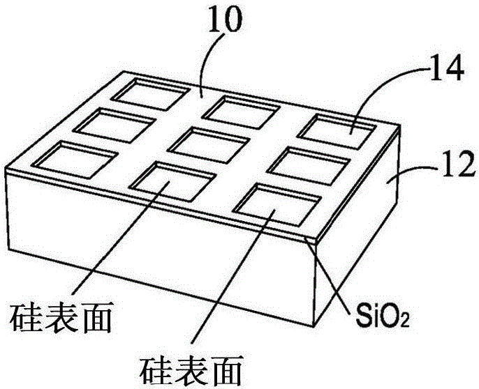
[0024] refer to Figure 2a to Figure 2e , a method for fabricating atomically flat (11-22) GaN templates on (113) silicon will now be described. First, a (113) silicon substrate, ie, a silicon substrate having a flat surface in the (113) plane of its crystal structure, is provided. like Figure 2a As shown, SiO was deposited on the surface of (113) silicon substrate 12 by plasma enhanced chemical vapor deposition (PECDV). 2 film10. In other embodiments, SiO can be deposited by electron beam evaporator or sputter deposition 2 . Then, if Figure 2b As shown, using standard photolithography and dry etching techniques (in this case, reactive ion etching RIE) 2 The film is etched through to an array of windows 14 (in this example, regular 2 x 2 μm sized square windows (although the window size could be larger) with about 1 μm spacing (although the spacing could be from 100 nm to 5 μm). Small or larger, square arrays from 500 x 500 nm to 10 x 10 μm) open across the wafer. Th...


PUM


Abstract

A method of growing a group III nitride crystal structure comprises: providing a silicon substrate(12); forming a first mask (10) on the substrate, the mask having a plurality of apertures (14) through it each exposing a respective area of the silicon substrate; etching the silicon exposed by each of the apertures to form a respective recess(16)having a plurality of facets(18, 20, 22, 24); depositing a second mask over some of the facets of each recess leaving at least one of the facets(22)of each recess exposed; and growing group III nitride on the exposed facets(22) and then over the substrate to form a continuous layer.

Description

technical field [0001] The present invention relates to the growth of non-polar and semi-polar crystal structures, and templates comprising such structures. It has particular application for growing semipolar or nonpolar GaN on silicon, but can also be used for other III-nitrides such as semipolar aluminum nitride (AlN), semipolar aluminum gallium nitride (AlGaN), or Semi-polar indium gallium nitride (InGaN). Background technique [0002] The past four decades have seen an unprecedented impact on the semiconductor industry generated by silicon technology, accounting for more than 90% of the global semiconductor market. Considering the mature and cost-effective silicon-based technologies, the combination of III-V and silicon technologies has the potential to provide a very good solution for the integration of electronics and photonics-based semiconductors. General lighting consumes 19% of total energy consumption worldwide. Due to the need for significantly increased energ...

Claims


Application Information

Patent Timeline
Patent Type & Authority Applications(China)
IPC IPC(8): H01L21/02
CPCH01L21/02639H01L21/02381H01L21/0243H01L21/02433H01L21/02458H01L21/0254H01L21/02609H01L21/02647H01L21/02658H01L21/308H01L29/2003
Inventor 王涛
Owner SEREN PHOTONICS
Why Eureka
Try Eureka