
Package structure and method for light emitting diodes

A technology of light-emitting diodes and packaging structures, which is applied in the direction of electrical components, electrical solid devices, circuits, etc., can solve problems such as short circuits, and achieve the effects of convenient use, saving processing costs, and reducing production costs

Inactive Publication Date: 2017-02-22
张宇顺
View PDF4 Cites 0 Cited by
  • Summary
  • Abstract
  • Description
  • Claims
  • Application Information

AI Technical Summary

Problems solved by technology

[0004] An object of the present invention is to propose a packaging structure of light-emitting diodes, which can solve the problem that the existing packaging structure of light-emitting diodes is easy to cause short circuit due to power trip, and greatly improves the use efficiency of the LED packaging structure

Method used


Image

  • Package structure and method for light emitting diodes
  • Package structure and method for light emitting diodes
  • Package structure and method for light emitting diodes

Examples


Embodiment 1

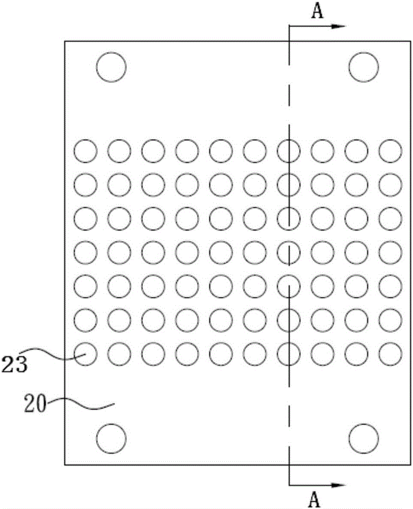
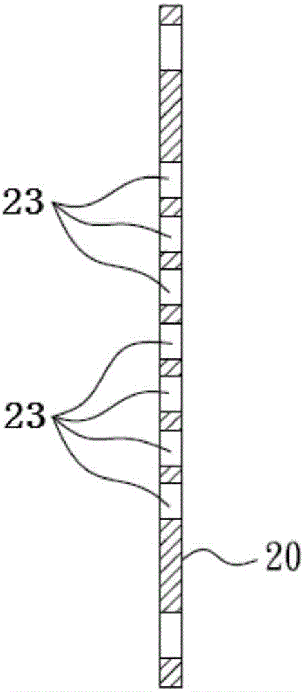
[0034] Such as Figure 1-Figure 4 As shown, this embodiment provides a preferred packaging structure of light emitting diodes, which includes a metal substrate 10, an insulating layer 20, an electrode layer 30, a plurality of LED chips 40, a plurality of bonding wires 50 and a plurality of Lens 60. Specifically, the metal substrate 10 has a front surface 11 and a back surface 12, wherein an insulating layer 20 is laminated on the front surface 11 of the metal substrate 10, the insulating layer 20 has a certain thickness, and a plurality of holes penetrating through the insulating layer 20 are opened on it. Through holes 23 on the front side 21 and the back side 22 . Here, a plurality of through holes 23 are arranged on the insulating layer 20 in an array, such as figure 2 Among them, the insulating layer 20 is provided with seven rows and ten columns of through holes 23, wherein the distance between two adjacent through holes 23 is equal, and the range of values ​​thereof i...

Embodiment 2

[0041] This embodiment proposes a packaging method suitable for the above light-emitting diode packaging structure, which specifically includes the following steps:

[0042] Step A: provide a metal substrate 10, and stick a plurality of LED dies 40 on its front surface 11;

[0043] Here, a plurality of LED dies 40 are arranged in an array on the front surface 11 of the metal substrate 10 , and specifically can be arranged in a rectangular array, a circular array, an elliptical array, a triangular array, etc. as required. Moreover, each LED die 40 is provided with a second electrode group 42 , and the second electrode group 42 includes a second positive electrode and a second negative electrode.

[0044] Step B: providing an insulating layer 20, on which a plurality of through holes 23 are formed to correspond to a plurality of LED chips 40 one-to-one;

[0045] In this step, the insulating layer 20 has a certain thickness, which is greater than that of the LED die 40 , so as t...


PUM


Abstract

The invention discloses a package structure for light emitting diodes and particularly relates to the technical field of semiconductor package. The package structure comprises a metal substrate. An insulation layer is formed on the metal substrate and provided with through holes. LED dies are arranged in the bottom of the through holes. An electrode layer for an external power supply is arranged above the insulation. The electrode layer is higher than the LED dies and connected to the LED dies via a connecting line. A filler material is used to fill in the through holes and to form a leans which encapsulates the LED die. The invention further discloses a package method for light emitting diodes. The package method is characterized in that there is a height difference between the electrode layer and the LED dies in ways that the electrode layer is arranged above the insulation, wherein the insulation is provided with the LED dies in the through holes. The method efficiently resolves the problem of short-circuit caused by the fact that the distance between the two ends of the connecting line is too close, accordingly the efficiency of the package structure for light emitting diodes is improved.

Description

technical field [0001] The invention relates to the technical field of semiconductor packaging, in particular to a packaging structure of a light emitting diode and a packaging method thereof. Background technique [0002] The existing LED package structure generally includes: heat dissipation substrate, insulating layer, SMD LED light-emitting chip, metal electrodes and lenses, among which each LED grain can be selected as a flip chip (Flip Chip) according to the process requirements. Or wire bond (Wire bond) is electrically connected to the heat dissipation substrate to complete the packaging of the LED. Afterwards, the above-mentioned LED packaging structure is fixedly connected to the heat sink of the light emitting device, and then the LED light emitting device is formed. Generally speaking, the heat dissipation substrate of the existing LED packaging structure is formed by sequentially laminating a circuit layer, an insulating layer and a substrate. When the LED chip...

Claims


Application Information

Patent Timeline
Patent Type & Authority Applications(China)
IPC IPC(8): H01L25/075H01L33/48H01L33/62H01L33/54H01L33/58H01L33/64
CPCH01L25/0753H01L33/486H01L33/54H01L33/58H01L33/62H01L33/64H01L2933/0058
Inventor 张宇顺
Owner 张宇顺
Learn More