


Quick Research
Generate reliable direction feasibility study reports for your R&D in just a few steps.

Technical Q&A
Discover and master advanced knowledge NOW. Basics, ideas, possibilities, all at once.

Find Solutions
As an expert in R&D theories, this can generate solutions to your technical problems instantly.

Evaluate Feasibility
Analyze your overall solution with one click, know your potential R&D risks in advance.

Monitor Landscape
Get weekly tech updates, stay abreast of the latest tech innovations and key insights.
Formation method of semiconductor structure
A semi-conductor and anti-penetration technology, which is applied in the direction of semiconductor devices, semiconductor/solid-state device manufacturing, electrical components, etc., can solve the problems of serious short channel effect and poor performance, and achieve the suppression of punch-through phenomenon, short channel effect suppression, and reliability sex enhancing effect
- Summary
- Abstract
- Description
- Claims
- Application Information
AI Technical Summary
Problems solved by technology
Method used
Image

Examples
Embodiment Construction
[0032] As mentioned in the background art, as the size of semiconductor devices shrinks and the degree of integration increases, the feature size of FinFETs also shrinks accordingly, making the short channel effect of FinFETs increasingly serious and poor in performance.
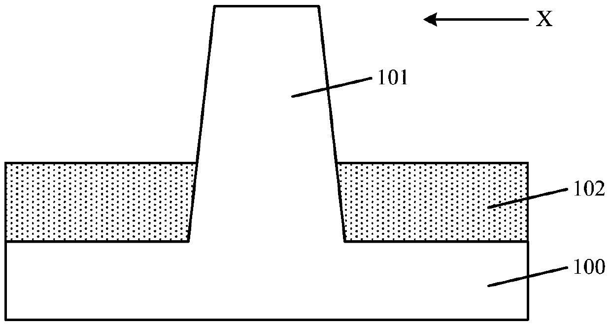
[0033] Please refer to figure 1 , figure 1 It is a schematic cross-sectional structure diagram of a fin for forming a fin field effect transistor according to an embodiment of the present invention, including: a substrate 100, a fin 101 located on the surface of the substrate 100, and an isolation layer 102 located on the surface of the fin 101. The isolation layer 102 covers part of the sidewall surface of the fin portion 101 , and the surface of the isolation layer 102 is lower than the top surface of the fin portion 101 .
[0034] Wherein, the base 100 and the fin 101 have well regions inside. When the FinFET is a PMOS transistor, the well is doped with N-type ions; when the FinFET is an NMOS transistor...
PUM
 Abstract
Description
Claims
Application Information
 - R&D Engineer
- R&D Manager
- IP Professional
- Industry Leading Data Capabilities
- Powerful AI technology
- Patent DNA Extraction
Browse by: Latest US Patents, China's latest patents, Technical Efficacy Thesaurus, Application Domain, Technology Topic, Popular Technical Reports.
© 2024 PatSnap. All rights reserved.Legal|Privacy policy|Modern Slavery Act Transparency Statement|Sitemap|About US| Contact US: help@patsnap.com