
Si-Sb-Se nano phase-change thin film material and preparation method and application thereof

A thin-film material, nano-phase technology, applied in metal material coating process, ion implantation plating, coating and other directions, can solve the problems of low melting point, volatile, and easy to contaminate semiconductors of Te material, and achieve high data retention capability, The effect of improving thermal stability and increasing storage speed

Inactive Publication Date: 2017-02-01
JIANGSU UNIV OF TECH
View PDF7 Cites 10 Cited by
  • Summary
  • Abstract
  • Description
  • Claims
  • Application Information

AI Technical Summary

Problems solved by technology

Traditional Ge 2 Sb 2 Te 5 The phase change material contains Te element. Te material has a low melting point, is volatile, and is toxic. It is easy to pollute the production line of the semiconductor industry and has adverse effects on the human body and the environment. All these hinder the industrialization of PCRAM.

Method used


Image

  • Si-Sb-Se nano phase-change thin film material and preparation method and application thereof
  • Si-Sb-Se nano phase-change thin film material and preparation method and application thereof
  • Si-Sb-Se nano phase-change thin film material and preparation method and application thereof

Examples


Embodiment 1

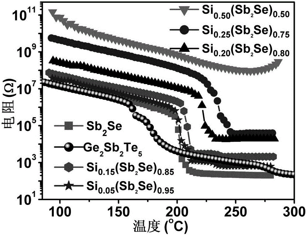
[0029] The structure of the Si-Sb-Se nano phase change thin film material prepared in this example is specifically Si 0.05 (Sb 2 Se) 0.95 .

[0030] The preparation steps are:

[0031] 1. Clean SiO2 2 / Si(100) substrate, cleaning the surface and back, removing dust particles, organic and inorganic impurities;

[0032] a) strong ultrasonic cleaning in acetone solution for 3-5 minutes, and rinse with deionized water;

[0033] b) Strong ultrasonic cleaning in ethanol solution for 3-5 minutes, rinse with deionized water, high-purity N 2 Blow dry the surface and back;

[0034] c) Dry the water vapor in an oven at 120°C for about 20 minutes.

[0035] 2. Preparation of Si by AC RF sputtering power supply 0.05 (Sb 2 Se) 0.95 Film preparation:

[0036] a) Install Sb 2 Se sputtering target, the Si sheet with a diameter of 6mm is stacked on the Sb 2 The center of the Se target constitutes a composite target. Sb 2 The purity of both Se and Si flakes reached 99.999% (atomic ...

Embodiment 2

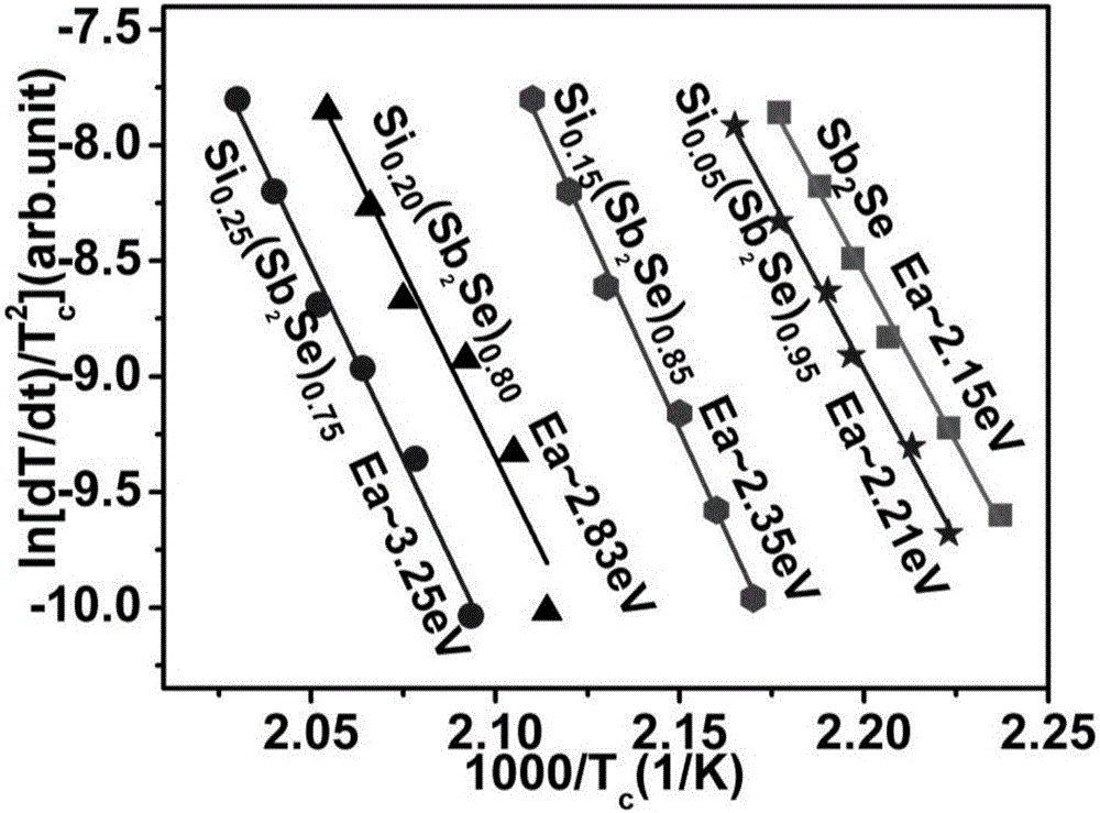
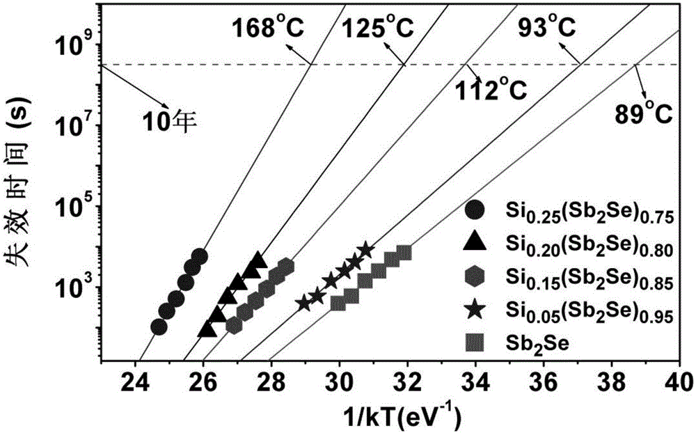
[0044] The specific structures of the Si-Sb-Se nano phase change thin film materials prepared in this example are Si 0.15 (Sb 2 Se) 0.85 、Si 0.20 (Sb 2 Se) 0.80 、Si 0.25 (Sb 2 Se) 0.75 , and the Si 0.15 (Sb 2 Se) 0.85 、Si 0.20 (Sb 2 Se) 0.80 、Si 0.25 (Sb 2 Se) 0.75 The thickness of the nano phase change film material is 50nm.

[0045] Above Si 0.15 (Sb 2 Se) 0.85 、Si 0.20 (Sb 2 Se) 0.80 、Si 0.25 (Sb 2 Se) 0.75 The preparation method of nanometer phase-change film material is identical with example 1, difference is in Sb 2 The diameters of the Si sheets stacked at the center of the Se target are 12 mm, 18 mm, and 24 mm, respectively.


PUM

PropertyMeasurementUnit
diameteraaaaaaaaaa
thicknessaaaaaaaaaa
thicknessaaaaaaaaaa

Abstract

The invention belongs to the field of semiconductor materials, and discloses an Si-Sb-Se nano phase-change thin film material. A general formula of a chemical composition of the phase-change thin film material is Si<x>(Sb<2>Se)<1-x>, wherein x is smaller than 0.50 and greater than or equal to 0.05; the proportion of an ingredient Si in the Si<x>(Sb<2>Se)<1-x> is controlled through the diameters of stacked Si sheets; and the Si-Sb-Se nano phase-change thin film material is formed by deposition through a room-temperature high-vacuum magnetron sputtering method. The Si-Sb-Se nano phase-change thin film material provided by the invention does not contain a Te element and belongs to an environment-friendly material; and meanwhile, Si-Sb-Se also has ultra-high thermal stability, relatively low power consumption and a high phase change speed, is an ideal phase-change storage material and has a relatively good market application prospect.

Description

technical field [0001] The invention relates to a semiconductor material in the technical field of microelectronics, in particular to a composite phase-change film material used for low-power, high-speed phase-change memory and its preparation and application. Background technique [0002] Phase-change memory (PCRAM) is a new type of non-volatile memory based on chalcogenide materials, which mainly utilizes the rapid conversion of materials between crystalline and amorphous states to realize information storage. Under the excitation of current pulses, the phase change material can realize the repeated conversion between the crystalline state and the amorphous state. When the phase change material is in the amorphous state, it has high resistance, and when it is in the crystalline state, it has low resistance. Huge differences serve as different data storage states to achieve the purpose of information storage. PCRAM has the advantages of strong stability, high storage densi...

Claims


Application Information

Patent Timeline
Patent Type & Authority Applications(China)
IPC IPC(8): H01L45/00C23C14/35C23C14/16C23C14/18
CPCC23C14/16C23C14/18C23C14/35H10N70/231H10N70/8825H10N70/026
Inventor 胡益丰朱小芹邹华张建豪孙月梅薛建忠吴世臣袁丽吴卫华郑龙翟良君
Owner JIANGSU UNIV OF TECH
Learn More