A kind of PD base variable capacitive hydrogen sensor and preparation method thereof
A variable capacitance and sensor technology, applied in the field of gas sensing, can solve the problems of complex manufacturing process and high cost, and achieve the effects of good selectivity, low cost and stable performance
- Summary
- Abstract
- Description
- Claims
- Application Information
AI Technical Summary
Problems solved by technology
Method used
Image
Examples
Embodiment 1
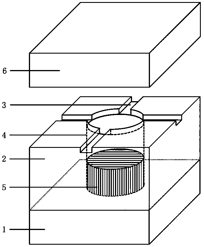
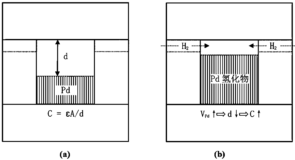
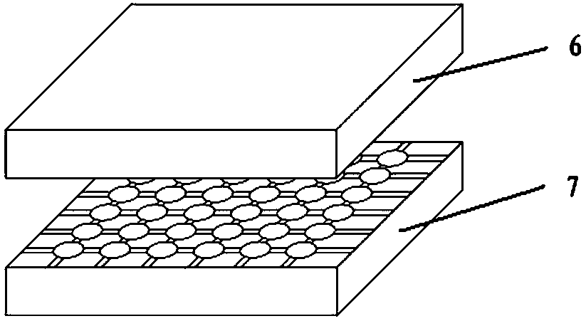
[0028] See attached figure 1 , which is a Pd-based variable capacitance hydrogen sensor provided by the present invention. The main components of the sensor include: resistivity between 10 -3 ~10 2 Ω·cm doped single crystal Si substrate 1, SiO grown by thermal oxidation 2 Layer 2, on SiO 2 Fabricate vent slots 3 on the SiO 2 Through-SiO 2 Layer deposition hole 4, Pd-based material 5 deposited in the deposition hole as the movable electrode of the sensor, and conductive flat material 6 as the static electrode of the sensor. Its specific structure is: thermal oxidation growth of SiO on doped single crystal Si substrate 1 2 Layer 2, SiO 2 The thickness of the layer is 0.5-1.5 microns; in SiO 2 through SiO 2 The deposition hole 4 of the layer, the movable electrode Pd-based material 5 is deposited in the deposition hole, and the height of the deposited movable electrode Pd-based material is SiO 2 50% to 90% of the layer thickness; in SiO 2 The upper surface of the layer...
Embodiment 2
[0039] The structure of the Pd-based variable capacitance hydrogen sensor provided in this embodiment is the same as that in Embodiment 1. The method of making the sensor is:
[0040] (1) A 1.5-micron-thick layer of SiO was grown on the surface of a 4-inch doped single-crystal Si wafer with a resistivity of 10 Ω cm by thermal oxidation 2 ;
[0041] (2) SiO grown by thermal oxidation by negative photolithography and hydrofluoric acid wet etching 2 Fabricated on a diameter of 1 cm and through the SiO 2 The deposition hole of the layer makes the conductive Si substrate exposed to the air;
[0042] (3) SiO grown by thermal oxidation using positive resist UV lithography and plasma etching processes 2 Make grid-shaped ventilation grooves with a depth of 0.2 microns;
[0043] (4) Using double-target co-sputtering supplemented by a stainless steel mask, selectively deposit 80%Pd / 20%Ni alloy in the deposition hole as the movable electrode of the sensor, and the height of the Pd-ba...
Embodiment 3
[0048] The structure of the Pd-based variable capacitance hydrogen sensor provided in this embodiment is the same as that in Embodiment 1. The method of making the sensor is:
[0049] (1) The thermal oxidation method is used at a resistivity of 5×10 -2 A layer of SiO with a thickness of 0.5 microns was grown on the surface of a 4-inch doped single-crystal Si substrate of Ω·cm 2 ;
[0050] (2) SiO grown by thermal oxidation using positive resist UV lithography and plasma etching processes 2 Make grid-shaped ventilation grooves with a depth of 0.1 microns;
[0051] (3) SiO grown by thermal oxidation by positive resist UV lithography and plasma etching 2 The upper fabrication diameter is 0.1 mm and runs through the SiO 2 The deposition hole of the layer makes the conductive Si substrate exposed to the air;
[0052] (4) Using double-target co-sputtering supplemented by a stainless steel mask, the pure 90%Pd / 10%Ag alloy is selectively deposited in the deposition hole as the m...
PUM
| Property | Measurement | Unit |
|---|---|---|
| electrical resistivity | aaaaa | aaaaa |
| thickness | aaaaa | aaaaa |
| height | aaaaa | aaaaa |
Abstract
Description
Claims
Application Information
 - R&D
- Intellectual Property
- Life Sciences
- Materials
- Tech Scout
- Unparalleled Data Quality
- Higher Quality Content
- 60% Fewer Hallucinations
Browse by: Latest US Patents, China's latest patents, Technical Efficacy Thesaurus, Application Domain, Technology Topic, Popular Technical Reports.
© 2025 PatSnap. All rights reserved.Legal|Privacy policy|Modern Slavery Act Transparency Statement|Sitemap|About US| Contact US: help@patsnap.com


