Fabrication method of low temperature poly-silicon array substrate, array substrate and display panel

A low-temperature polysilicon and array substrate technology, used in semiconductor/solid-state device manufacturing, gaseous chemical plating, coating, etc., can solve the problems of many processes, increase the cost and complexity of the manufacturing process, achieve uniform doping and reduce mask times, the effect of improving electrical performance

Inactive Publication Date: 2017-01-11
WUHAN CHINA STAR OPTOELECTRONICS TECH CO LTD
View PDF2 Cites 10 Cited by
  • Summary
  • Abstract
  • Description
  • Claims
  • Application Information

AI Technical Summary

Problems solved by technology

[0003] In the manufacturing process of the LTPS array substrate, when performing doping, the polysilicon layer is generally formed first, and then the channel doping, N-type doping, and P-type doping are performed. Not only the operation process is too complicated due to many processes, but also , each doping must go through a photomask, which increases the cost of the entire manufacturing process

Method used


Image

  • Fabrication method of low temperature poly-silicon array substrate, array substrate and display panel
  • Fabrication method of low temperature poly-silicon array substrate, array substrate and display panel
  • Fabrication method of low temperature poly-silicon array substrate, array substrate and display panel

Examples


Embodiment Construction

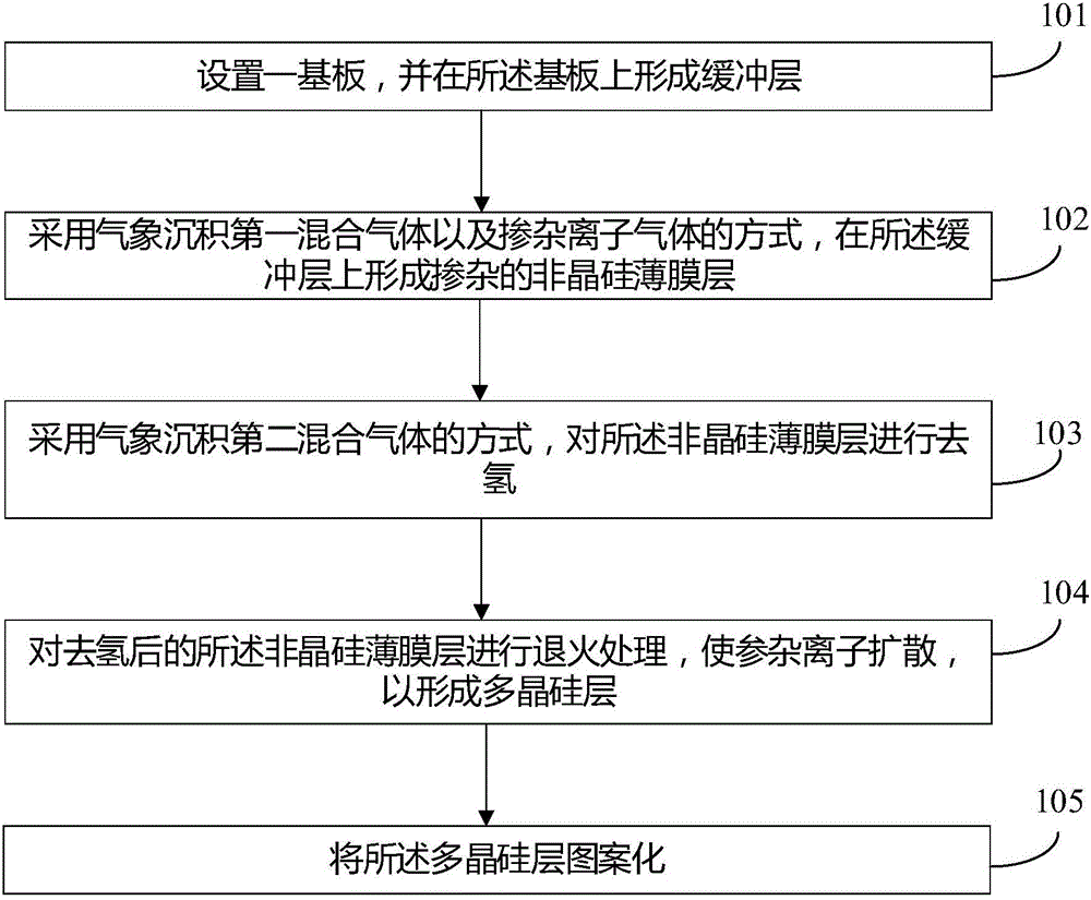
[0044] refer to figure 1 , figure 1 It is a schematic flow chart of an embodiment of the method for preparing a low-temperature polysilicon array substrate of the present invention. see also Figure 2A ~ Figure 2E The structure diagram of the corresponding low-temperature polysilicon array substrate, the manufacturing method of this embodiment includes the following steps:

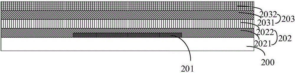
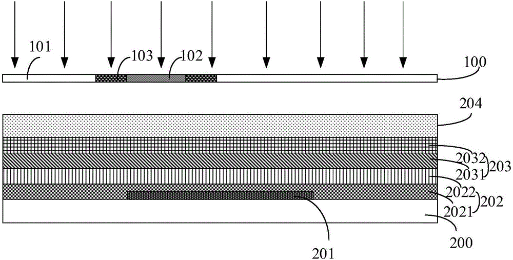
[0045] 101 : Setting a substrate 200 and forming a buffer layer 202 on the substrate 200 .

[0046] Wherein, the substrate 200 includes a glass substrate, and may also be other substrates such as a quartz substrate in other embodiments, which is not limited here.

[0047] Specifically, first set the first substrate 200, first form the light-shielding layer 201 on the first substrate 200, then deposit the SiNx layer 2021 on the light-shielding layer, and then deposit the SiOx layer 2022 on the SiNx layer 2021, wherein the SiNx layer 2021 and the SiOx layer 2022 constitute the buffer layer 202 .

[0048...


PUM


Abstract

The invention discloses a fabrication method of a low temperature poly-silicon array substrate, the array substrate and a display panel. The fabrication method comprises the steps of arranging a substrate, and forming a buffer layer on the substrate; forming a doped amorphous silicon film layer on the buffer layer by a mode of vapor deposition of a first mixed gas and a doped ion gas; dehydrogenizing the amorphous silicon film layer by a mode of vapor deposition of a second mixed gas; annealing the dehydrogenized amorphous silicon film layer so that doped ions are diffused to form a poly-silicon layer; and patterning the poly-silicon layer. By the fabrication method, the fabrication process of the low temperature poly-silicon array substrate can be effectively reduced, the investment of fabrication equipment is reduced, and the fabrication cost is further reduced.

Description

technical field [0001] The invention relates to the field of liquid crystal display, in particular to a method for preparing a low-temperature polysilicon array substrate, the array substrate and a display panel. Background technique [0002] With low temperature polysilicon technology LTPS (Low Temperature Poly-silicon) is currently developing rapidly, its biggest advantage lies in ultra-thin, light weight, low power consumption, can provide more vivid colors and clearer images. [0003] In the manufacturing process of the LTPS array substrate, when performing doping, the polysilicon layer is generally formed first, and then the channel doping, N-type doping, and P-type doping are performed. Not only the operation process is too complicated due to many processes, but also , each doping must go through a photomask, which increases the cost of the entire manufacturing process. Contents of the invention [0004] The technical problem mainly solved by the present invention i...

Claims


Application Information

Patent Timeline
Patent Type & Authority Applications(China)
IPC IPC(8): H01L21/77H01L27/12G02F1/1362C23C16/44H01L21/324
CPCC23C16/44G02F1/1362H01L21/324H01L21/77H01L27/12H01L27/1214H01L27/1259H01L2021/775H01L21/02422H01L21/02488H01L21/02532H01L21/02576H01L21/02579H01L21/02592H01L21/0262H01L21/02686H01L27/127H01L27/1285H01L27/1288H01L29/66757H01L29/78603H01L29/78633H01L29/78675G02F1/136209G02F1/1368G02F2202/104G02F1/13685H01L21/02672H01L21/02675H01L21/2254H01L27/1222
Inventor 郝晓丹殷婉婷
Owner WUHAN CHINA STAR OPTOELECTRONICS TECH CO LTD
Why Eureka
Try Eureka