
GGNMOS (Gate-Grounded N-channel Metal Oxide Semiconductor) device applied to ESD (Electro-Static discharge) protection and manufacturing method thereof

A technology of ESD protection and manufacturing method, applied in semiconductor/solid-state device manufacturing, semiconductor devices, electrical components, etc., can solve problems such as unfavorable heat dissipation, melting of gate oxide layer 13, device failure, etc., to improve ESD protection capability, The effect of improving secondary breakdown current and increasing uniformity

Active Publication Date: 2017-01-04
SHANGHAI HUALI MICROELECTRONICS CORP
View PDF3 Cites 3 Cited by
  • Summary
  • Abstract
  • Description
  • Claims
  • Application Information

AI Technical Summary

Problems solved by technology

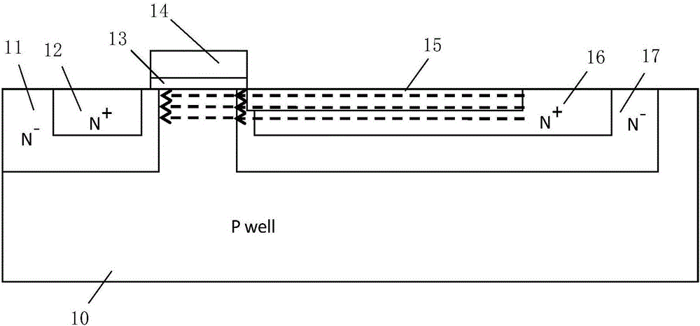
[0003] However, in the above structure, since the current during ESD leakage mainly flows on the surface of the drain diffusion region (draindiffusion) and the channel (channel) (as indicated by the arrow in the figure), and the thermal conductivity of silicon is Gate oxide is hundreds of times, so the gate oxide layer 13 (Gate oxide) is a poor conductor of heat, and the silicon substrate 10 (substrate silicon) is relatively a good conductor of heat, so the closer the ESD conduction current is to the drain terminal The surface of the diffusion region and the surface of the channel are more unfavorable to the dissipation of the heat generated by the ESD discharge current, so it is easier to cause the melting of the gate oxide layer 13 and cause various failures of the device

Method used


Image

  • GGNMOS (Gate-Grounded N-channel Metal Oxide Semiconductor) device applied to ESD (Electro-Static discharge) protection and manufacturing method thereof
  • GGNMOS (Gate-Grounded N-channel Metal Oxide Semiconductor) device applied to ESD (Electro-Static discharge) protection and manufacturing method thereof

Examples


Embodiment Construction

[0026] The specific embodiment of the present invention will be further described in detail below in conjunction with the accompanying drawings.

[0027] It should be noted that, in the following specific embodiments, when describing the embodiments of the present invention in detail, in order to clearly show the structure of the present invention for the convenience of description, the structures in the drawings are not drawn according to the general scale, and are drawn Partial magnification, deformation and simplification are included, therefore, it should be avoided to be interpreted as a limitation of the present invention.

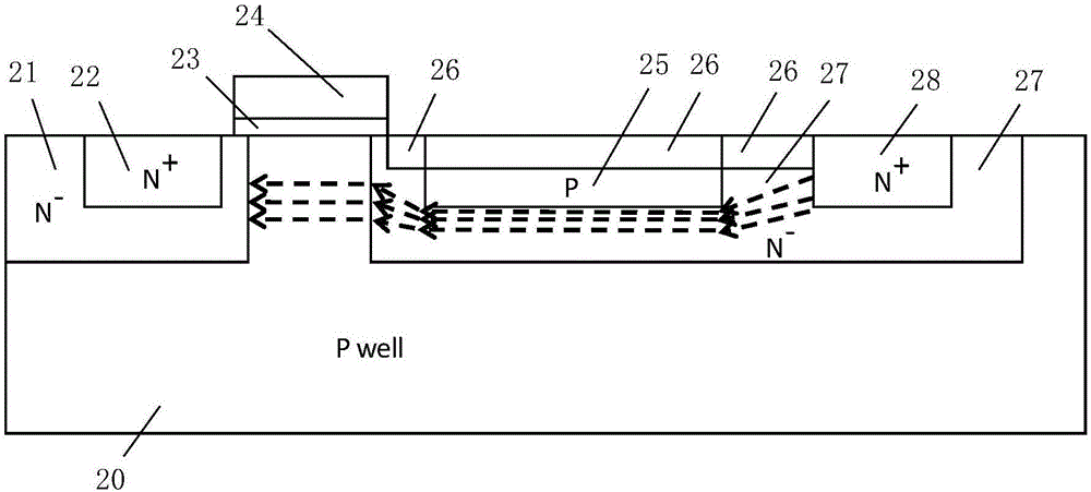
[0028] In the following specific embodiments of the present invention, please refer to figure 2 , figure 2 It is a schematic diagram of the structure of a GGNMOS device used for ESD protection in a preferred embodiment of the present invention. Such as figure 2 As shown, a GGNMOS (gate grounded NMOS) device used as ESD protection of the present...


PUM


Abstract

The invention discloses a GGNMOS (Gate-Grounded N-channel Metal Oxide Semiconductor) device applied to ESD (Electro-Static discharge) protection and a manufacturing method thereof. A P-type doping region is arranged in a drain extension region of a GGNMOS to form a floating reverse diode with a drain NLDD (N-type Lightly Doped Drain) doping region, so that distribution of drain ESD current is changed; ESD leakage current is deviated from the surface of the drain extension region and a conducting channel; the cooling capability during ESD discharge of the GGNMOS is enhanced; secondary breakdown current during snapback of the device is increased; and the ESD protection capability of the GGNMOS device is enhanced.

Description

technical field [0001] The invention relates to the technical field of manufacturing semiconductor integrated circuits, and more particularly, to a GGNMOS device used for ESD protection and a manufacturing method thereof. Background technique [0002] see figure 1 , figure 1 It is an existing GGNMOS device for ESD protection. Such as figure 1 As shown, the GGNMOS device is formed on a semiconductor silicon substrate 10, which has a gate (Gate) 14 and N-type doped source terminals (Source) 11 and 12 and a drain terminal (Drain) 17 located on both sides of the gate. and 16. In existing GGNMOS (gate grounded NMOS) devices used for ESD (electrostatic discharge) protection, in order to improve the ESD leakage capability of GGNMOS devices, an asymmetric source and drain structure is usually used in GGNMOS devices, that is, the drain terminal Do extension treatment, and add non-metallic silicide region 15 (silicide blocking) in the drain extension region (drain extension) to i...

Claims


Application Information

Patent Timeline
Patent Type & Authority Applications(China)
IPC IPC(8): H01L27/088H01L29/417H01L29/78H01L21/336
CPCH01L27/088H01L29/41725H01L29/66409H01L29/78
Inventor 朱天志颜丙勇
Owner SHANGHAI HUALI MICROELECTRONICS CORP
Learn More