
Low-scattering covering for external field testing and preparation method thereof

An external field testing, low-scattering technology, applied in chemical instruments and methods, lamination, layered products, etc., can solve the problems of not considering the delamination of the adhesive layer, only considering the reflectivity of the material, loss of electromagnetic waves, etc. Good site layout quickly, achieve designability, and ensure the effect of bond strength

Inactive Publication Date: 2017-01-04
SHANGHAI RADIO EQUIP RES INST
View PDF10 Cites 4 Cited by
  • Summary
  • Abstract
  • Description
  • Claims
  • Application Information

AI Technical Summary

Problems solved by technology

The materials used in traditional wave-absorbing patches are mainly wave-absorbing particles and adhesives, and there is less consideration for shielding performance. In addition, there is little consideration for the matching between the ground as the bottom material and the wave-absorbing patch; such as the patent CN102977480A discloses a method for preparing a rubber-based flexible wave-absorbing material, which is mainly aimed at the field of civil wave-absorbing materials. The method used is to fill the filler with the rubber according to a certain mass ratio, add an organic solvent during the mixing process, and knead After the completion, place it for a period of time, and then roll it after the organic solvent evaporates to prepare a wave-absorbing patch. This type of patch is mainly wave-absorbing, and the shielding performance is insufficient. At the same time, the structure is simple, and it is difficult to achieve broadband wave-absorbing / shielding performance.
Patent CN104979641A proposes a broadband absorber with a sandwich structure, with a high-dielectric thin layer in the middle and composite loss layers with a thickness of 0.1-0.3 mm on both sides. The absorber can achieve two absorption peaks. Broadband absorption can be obtained after design, but this material only considers the reflectivity of the material, and does not analyze the shielding performance, nor does it consider the case where the substrate is the ground
Patent CN104893605A proposes a wave-absorbing sheet for electromagnetic shielding, including a graphite sheet as a reflective layer, a wave-absorbing layer and a release material layer, a first adhesive layer is arranged between the graphite sheet and the wave-absorbing layer, and the wave-absorbing layer There is a second adhesive layer between the release material layer. This structure uses a wave-absorbing material to achieve the shielding effect. The wave-absorbing performance is limited (only 88% at most), and the shielding performance is insufficient. The adhesive layer is not considered. Delamination occurs under stress
In addition, the research on shielding materials usually focuses on the reflection of electromagnetic waves. The prepared materials are usually conductive or semi-conductive structures, which cannot eliminate clutter, and sometimes secondary reflection or electromagnetic coupling may occur. Phenomenon, such as patent CN105246315A provides a kind of preparation method of flexible shielding material, the substrate film is placed in conductive glue, sizing and then dried to obtain conductive film, the substrate film used is selected from mesh film or grid cloth, Then vacuum coating is adopted, and a metal film and a metal protective film are sequentially plated on the surface of the conductive film to obtain a flexible shielding material. This structure can reflect electromagnetic waves better, and the shielding performance is better. However, considering the coating process in the base film The volume is small, and the conductive film on the surface may be damaged and the shielding performance may be reduced under multiple folds.
Patent CN105218953A discloses a semi-conductive insulating shielding material for ethylene-propylene rubber cables. The volume resistivity of the prepared semi-conductive shielding layer at 20°C is 50-90Ω·cm, which has good shielding performance, mechanical properties, and Aging and other properties, but it does not have the absorption function for electromagnetic waves
Patent CN105131612A proposes a self-adhesive conductive silicone rubber electromagnetic shielding material. The electromagnetic shielding material is composed of silicone rubber, tackifier, coupling agent, vulcanizing agent, and functional filler according to weight percentage. The functional filler is conductive conductive Conductive particles of carbon black, nickel-coated graphite, nickel-coated glass beads, silver-aluminum powder, silver-coated glass beads, etc., have an average particle size of 0.01 to 500 microns, although the material has the function of conductive electromagnetic shielding and self-adhesive characteristics, but it also does not have the function of loss of electromagnetic waves, so it cannot be used in field tests

Method used


Image

  • Low-scattering covering for external field testing and preparation method thereof
  • Low-scattering covering for external field testing and preparation method thereof
  • Low-scattering covering for external field testing and preparation method thereof

Examples

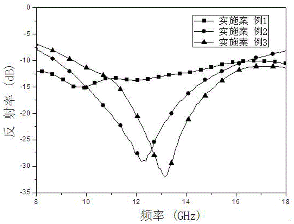

preparation example Construction

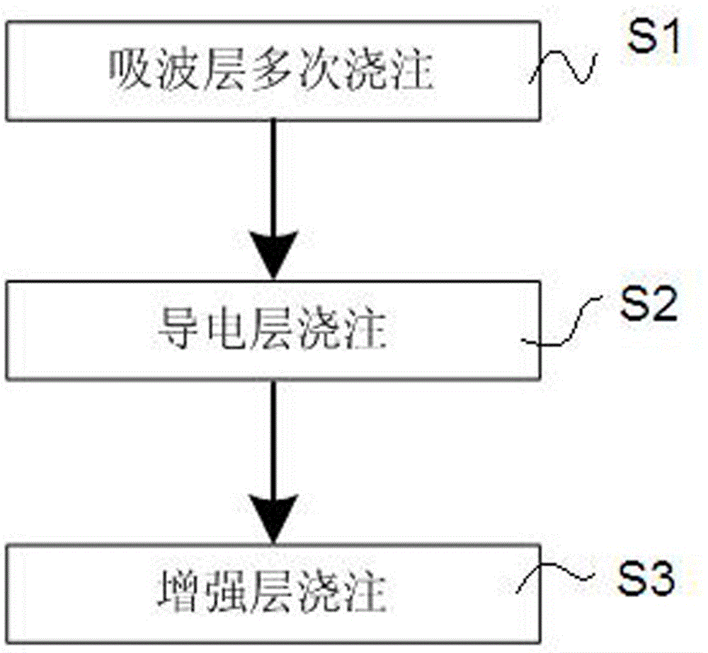
[0043] The preparation method of the low-scattering covering for field testing provided by the invention comprises the following steps, such as figure 2 Shown:

[0044] Step 1 (S1): Multi-layer absorbing material casting process to prepare the absorbing layer

[0045] Spherical or sheet-shaped carbonyl iron particles and rubber are filled at a volume addition ratio of 5-50%. The bottom absorbing layer is a mixture of sheet-shaped carbonyl iron and room temperature curing silicone rubber materials. Coupling agent (such as silane coupling agent KH550, KH560, etc.) with iron powder mass ratio of 1-2%, until mixed evenly, then add curing agent for room temperature curing silicone rubber filler (such as epoxy silane crosslinking agent), mass The ratio is 5% of the rubber. After adding the curing agent and mixing evenly, pour it into the predetermined plane cavity. When the rubber material reaches the semi-cured state, configure the second layer of material, the additive is spher...

Embodiment 1

[0053] ① The first layer of absorbing material is a mixture of spherical carbonyl iron with a volume addition ratio of 20% and room temperature curing silicone rubber material, and the thickness of the planar cavity is set to 0.43mm;

[0054] ②For the second layer of absorbing material, the additive is sheet-shaped carbonyl iron particles, the volume addition ratio is 20%, and the thickness of the planar cavity is set to 0.77mm;

[0055] ③For the third layer of absorbing material, the additive is sheet-shaped carbonyl iron particles, the volume addition ratio is 45%, and the thickness of the planar cavity is set to 0.4mm;

[0056] ④ For the fibers in the middle conductive layer, the average length is 3 mm, the average diameter is 20 μm, the average length-to-diameter ratio is 150, the volume ratio is 30%, and the thickness of the prepared material is 2 mm.

[0057] ⑤ For the bottom reinforcement layer, the thickness of both layers of rubber is 1mm, the mesh size of the mesh cl...

Embodiment 2

[0059] ① The first wave-absorbing layer is a mixture of sheet-shaped carbonyl iron with a volume addition ratio of 10% and room temperature curing silicone rubber material, and the thickness of the planar cavity is set to 1.5mm;

[0060] ②For the second layer of absorbing material, the additive is spherical carbonyl iron particles, the volume addition ratio is 15%, and the thickness of the planar cavity is set to 0.5mm;

[0061] ③For the fibers in the middle conductive layer, select the average length of 2mm, the average diameter of 20μm, the average aspect ratio of 100, the addition ratio is 40% by volume, and the thickness of the prepared material is 2mm.

[0062] ④ For the bottom reinforcement layer, the thickness of both layers of rubber is 1.5mm, the mesh size of the mesh cloth laid in the middle is 15mm, and the fiber is glass fiber mesh cloth. Example 3:


PUM

PropertyMeasurementUnit
Thicknessaaaaaaaaaa
Thicknessaaaaaaaaaa
Thicknessaaaaaaaaaa

Abstract

The invention discloses a low-scattering covering for external field testing and a preparation method thereof. The low-scattering covering comprises a wave absorbing layer, a conducting layer and a reinforcing layer; the wave absorbing layer comprises a plurality layers of wave absorbing material, and the wave absorbing material is formed by adding wave absorbing microparticles into a silicone rubber material; the conducting layer is formed by adding conducting fibers into a silicone rubber material; a built-in fiber mesh cloth structure is adopted by the reinforcing layer, and fiber mesh cloth is arranged between the two silicone rubber material layers. According to the low-scattering covering for external field testing and the preparation method thereof, multiple layers of wave absorbing material are prepared by mixing liquid rubber with the wave absorbing microparticles, the conducting fibers, a reinforcing material and the like in a multi-time pouring mode. A material prepared from the covering can be applied to electromagnetic scattering testing of a large target in an external field to achieve the good electromagnetic wave absorbing or shielding effect, has the advantages of being high in field arrangement speed, resistant to oxidization and corrosion, low in manufacturing cost and the like and is a complex wave absorbing or shielding electromagnetic product with the application prospect.

Description

technical field [0001] The present invention relates to the manufacture of wave-absorbing and shielding materials with complex structures. Specifically, it relates to a low-scattering covering for field testing, which can reduce background electromagnetic waves after shielding for civilian or military electronic equipment or target field testing. Scattering and electromagnetic coupling between the background and the target, thereby reducing the influence of the background on the target test. Background technique [0002] With the development of electromagnetic testing technology, the electromagnetic scattering characteristic test of the target is very important to improve the survivability of the target and the accuracy of positioning judgment. For the field test target, the radar cross section (radar cross section, RCS) of the target is one of the important indicators reflecting its performance characteristics. With the increasing demand for testing low-scattering targets ...

Claims


Application Information

Patent Timeline
IPC IPC(8): B32B25/20B32B25/02B32B25/10B32B25/04B32B25/08B32B3/12B32B37/02
CPCB32B25/20B32B3/12B32B25/02B32B25/04B32B25/08B32B25/10B32B37/02B32B2260/021B32B2260/025B32B2260/048B32B2307/212B32B2307/714B32B2307/752
Inventor 许勇刚梁子长王晓冰袁黎明
Owner SHANGHAI RADIO EQUIP RES INST
Learn More