Xilinx-FPGA-based multi-gigabit-network flow combination system and realization method thereof
An implementation method and network port technology, applied in the field of network communication, can solve the problems of high hardware cost and software cost, unable to meet the various needs of users, etc. Effect
- Summary
- Abstract
- Description
- Claims
- Application Information
AI Technical Summary
Problems solved by technology
Method used
Image
Examples
Embodiment 1
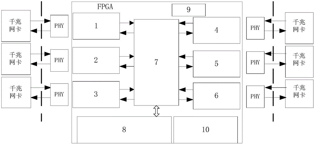
[0064] The embodiment of the present invention discloses a method for realizing multi-gigabit network convergence based on Xilinx FPGA, see figure 1 , the Xilinx FPGA-based multi-gigabit network convergence system consists of the following parts: the first MAC module 1, the second MAC module 2, the third MAC module 3, the fourth MAC module 4, the fifth MAC module 5, and the sixth MAC module Module 6, internal processing logic module 7, PCIE high-speed interface module 8, clock module 9, and other external interface logic modules 10.
[0065] see figure 2 , the first MAC module 1 includes: a first gigabit ETMAC core module 11, a first RGMII interface module 12, a first transceiver processing logic module 13, and a first synchronization module 14, which are used to establish a gigabit network for data transceiving .
[0066] The first transceiver processing logic module 13 includes: a first TX module 131 and a first RX module 132 , the first TX module 131 is used for data tra...
Embodiment 2
[0078] The embodiment of the present invention discloses an implementation method of a Xilinx FPGA-based multi-gigabit network convergence system, see Figure 5 , the implementation method includes the following steps:
[0079] 101: After the system is started, the first MAC module 1, the second MAC module 2, the third MAC module 3, the fourth MAC module 4, the fifth MAC module 5, and the sixth MAC module 6 are initialized, and the six MAC modules are respectively Configure the corresponding PHY module accordingly, such as MAC address, flow control settings, etc.;
[0080] 102: Configure the external PHY register through the MDIO (management data interface) bus interface to meet the needs of MAC communication;
[0081] 103: Complete the initialization of the PCIE high-speed interface module 8;
[0082] Wherein, this step is the same as the operation process of step 101, which is not repeated in this embodiment of the present invention.
[0083] 104: The system checks that t...
Embodiment 3
[0088] Combine below Figure 6 The data communication from the network port to the host direction of the implementation method of the Xilinx FPGA-based multi-gigabit network confluence system in embodiment 2 is described in detail, and the first MAC module 1 is used as an example for illustration, see the following description for details:
[0089] 201: The network port receives data, after being processed by the first RX module 132, it enters the bus receiving buffer with an 8-bit width, and generates a data fetch flag every time a frame is full, and notifies the bus to fetch data;
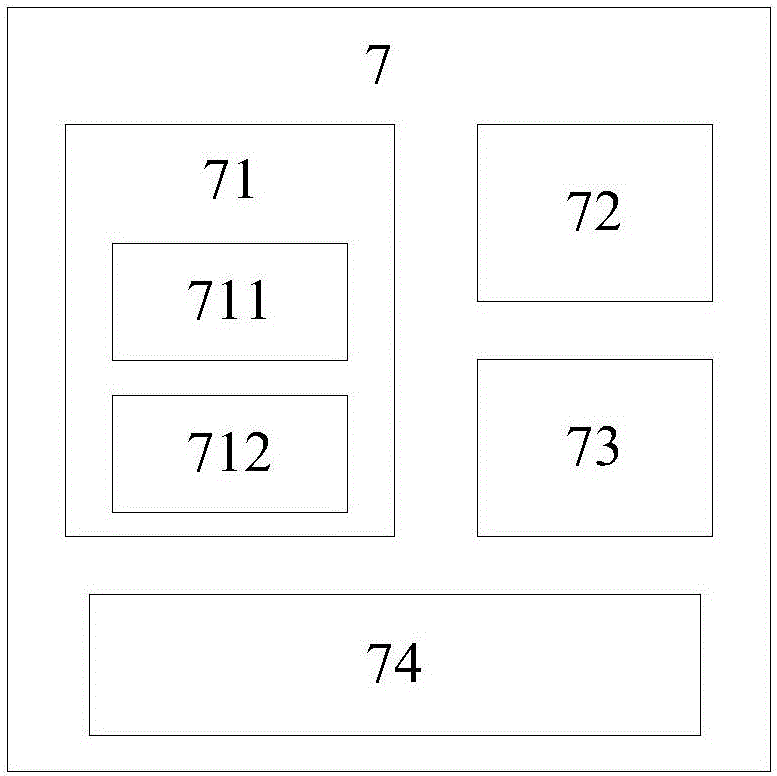
[0090] 202: The receiving bus module 711 extracts data frames from the receiving buffer of the first RX module 132 packet by packet according to the order in which the data arrives, and performs parsing, filtering and other related processing through the data processing module 74;
[0091] 203: The receiving bus module 711 forms a large packet of the processed related network frames and transfers...
PUM
 Abstract
Description
Claims
Application Information
 - R&D Engineer
- R&D Manager
- IP Professional
- Industry Leading Data Capabilities
- Powerful AI technology
- Patent DNA Extraction
Browse by: Latest US Patents, China's latest patents, Technical Efficacy Thesaurus, Application Domain, Technology Topic, Popular Technical Reports.
© 2024 PatSnap. All rights reserved.Legal|Privacy policy|Modern Slavery Act Transparency Statement|Sitemap|About US| Contact US: help@patsnap.com


