Transparent circuit board
A transparent circuit board, transparent conductive technology, used in transparent dielectrics, circuit substrate materials, printed circuits, etc.
- Summary
- Abstract
- Description
- Claims
- Application Information
AI Technical Summary
Problems solved by technology
Method used
Image

Examples
Embodiment 1
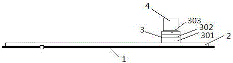
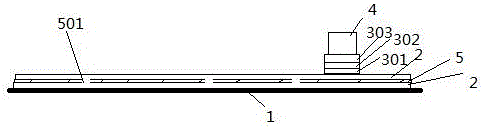
[0021] Such as figure 1 As shown, the transparent circuit board of the present invention has a transparent conductive substrate 1, the transparent conductive substrate is a conductive transparent substrate with a square resistance of less than 35Ω, a layer of circuit 2 is provided on the transparent conductive substrate 1, and a layer of circuit 2 is provided on the circuit 2. The electrode 3 of the circuit layer is formed by sputtering two metal material layers.
[0022] Wherein, the first metal material layer 301 is one or more alloys of molybdenum and niobium, with a thickness of 5-100 nanometers.
[0023] The second metal material layer 302 is metal copper with a thickness of 10-300 nanometers.
[0024] The third metal material layer 303 is an alloy of nickel and rare earth elements, with a thickness of 30-500 nanometers.
[0025] A 10-20 μm metal transmission signal line is arranged on the transparent substrate, and the metal transmission signal line is fixed on the sam...
Embodiment 2
[0027] Such as figure 1 As shown, the transparent circuit board of the present invention has a transparent conductive substrate 1, the transparent conductive substrate is a conductive transparent substrate with a square resistance of less than 35Ω, a layer of circuit 2 is provided on the transparent conductive substrate 1, and a layer of circuit 2 is provided on the circuit 2. The electrode 3 of the circuit layer is formed by sputtering two metal material layers.
[0028] Wherein, the first metal material layer 301 is molybdenum with a thickness of 5-100 nanometers.
[0029] The second metal material layer 302 is metal copper with a thickness of 10-300 nanometers.
[0030] The third metal material layer 303 is nickel or an alloy of nickel and rare earth elements, with a thickness of 30-500 nanometers.
[0031] A 10-20 μm metal transmission signal line is arranged on the transparent substrate, and the metal transmission signal line is fixed on the same metal material layer as...
Embodiment 3
[0033] Such as figure 1 As shown, the transparent circuit board of the present invention has a transparent conductive substrate 1, the transparent conductive substrate is a conductive transparent substrate with a square resistance of less than 35Ω, a layer of circuit 2 is provided on the transparent conductive substrate 1, and a layer of circuit 2 is provided on the circuit 2. The electrode 3 of the circuit layer is formed by sputtering two metal material layers.
[0034] Wherein, the first metal material layer 301 is one or two alloys of molybdenum and niobium, and the thickness is 5-100 nanometers.
[0035] The second metal material layer 302 is one or more alloys of copper, nickel, titanium and alloys of rare earth elements, with a thickness of 10-300 nanometers.
[0036] A 10-20 μm metal transmission signal line is arranged on the transparent substrate, and the metal transmission signal line is fixed on the same metal material layer as the circuit electrode.
PUM
| Property | Measurement | Unit |
|---|---|---|
| Square resistance | aaaaa | aaaaa |
| Thickness | aaaaa | aaaaa |
| Thickness | aaaaa | aaaaa |
Abstract
Description
Claims
Application Information
 - R&D
- Intellectual Property
- Life Sciences
- Materials
- Tech Scout
- Unparalleled Data Quality
- Higher Quality Content
- 60% Fewer Hallucinations
Browse by: Latest US Patents, China's latest patents, Technical Efficacy Thesaurus, Application Domain, Technology Topic, Popular Technical Reports.
© 2025 PatSnap. All rights reserved.Legal|Privacy policy|Modern Slavery Act Transparency Statement|Sitemap|About US| Contact US: help@patsnap.com