Humidity sensor based on organic field effect transistor and preparing method thereof
A technology of humidity sensor and transistor, applied in the direction of instruments, scientific instruments, measuring devices, etc., can solve the problems of poor flexibility, environmental pollution, low sensitivity, etc., and achieve the effects of strong flexibility, solving secondary pollution, and simple preparation process
- Summary
- Abstract
- Description
- Claims
- Application Information
AI Technical Summary
Problems solved by technology
Method used
Image
Examples
Embodiment 1
[0038] The preparation method is as follows:
[0039] ① Thoroughly clean the PI substrate sputtered with 50nm ITO as the gate electrode, and dry it with dry nitrogen after cleaning;
[0040] ② Prepare a PS film on ITO by spin coating to form a gate insulating layer of 100nm;
[0041] ③The spin-coated PS film is heated and baked;
[0042] 4. Spin coating indigo on the grid insulating layer: the organic semiconductor layer 100nm of bacterial cellulose nanofiber mass ratio is 97:3;
[0043] ⑤ Vacuum evaporation is used to prepare 80nm copper source electrodes and drain electrodes.
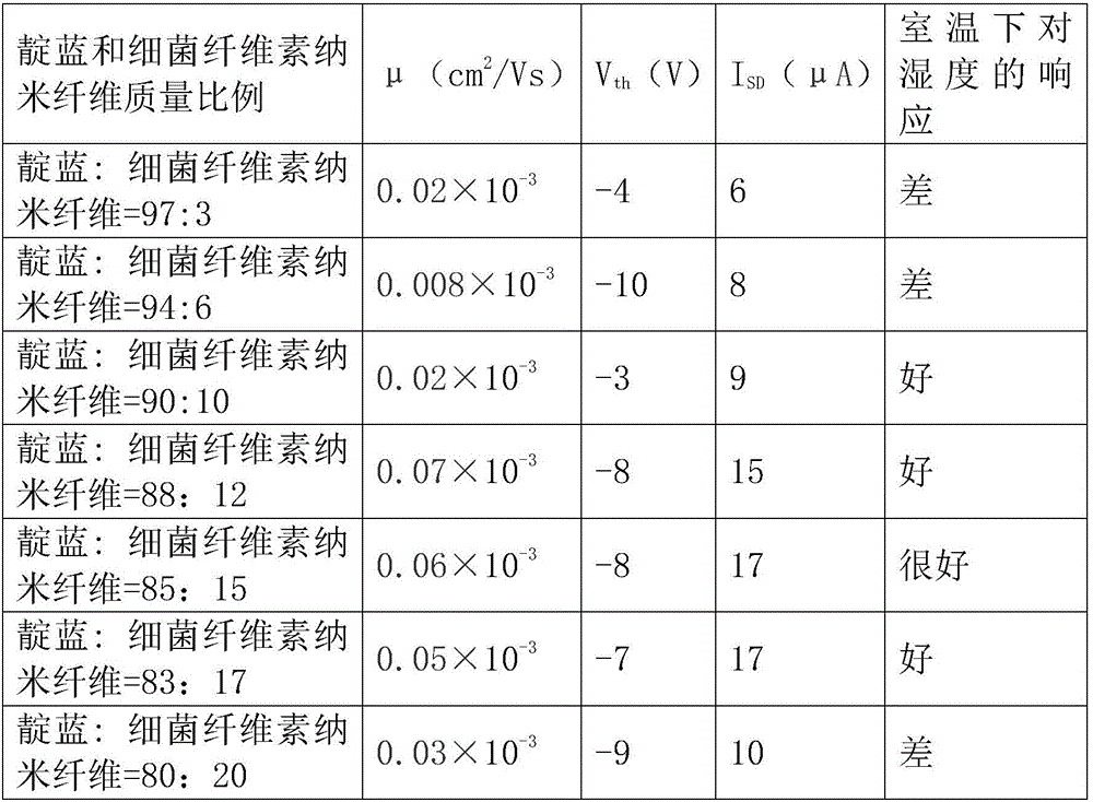
[0044] The humidity response characteristics of the device are tested, and the saturation current I of the device is measured SD =6μA, carrier mobility μ=0.02×10 -3 cm 2 / Vs, threshold voltage V TH = -4V, poor response to humidity at room temperature
Embodiment 2
[0046] The preparation method is as follows:
[0047] ① Thoroughly clean the PEI substrate sprayed with 80nm silver nanowires as the gate electrode, and dry it with dry nitrogen after cleaning;
[0048]② Prepare a PMMA film on the silver nanowire by spin coating method to form a gate insulating layer of 520nm;
[0049] ③Heating and baking the spin-coated PMMA film;
[0050] 4. Spin coating indigo on the grid insulating layer: the organic semiconductor layer 120nm of bacterial cellulose nanofiber mass ratio is 94:6;
[0051] ⑤ Vacuum evaporation is used to prepare silver source electrode and drain electrode 70nm.
[0052] The humidity response characteristics of the device are tested, and the saturation current I of the device is measured SD =8μA, carrier mobility μ=0.008×10 -3 cm 2 / Vs, threshold voltage V TH =-10V, poor response to humidity at room temperature.
Embodiment 3
[0054] The preparation method is as follows:
[0055] ① Thoroughly clean the shellac substrate sputtered with 70nm ITO as the gate electrode, and dry it with dry nitrogen after cleaning;
[0056] ② Prepare a PVA film on ITO by spin coating method to form a 20nm gate insulating layer;
[0057] ③The spin-coated PVA film is heated and baked;
[0058] 4. Spin coating indigo on the grid insulating layer: the organic semiconductor layer 100nm of bacterial cellulose nanofiber mass ratio is 90:10;
[0059] ⑤ Prepare gold source electrode and drain electrode 50nm by vacuum evaporation.
[0060] The humidity response characteristics of the device are tested, and the saturation current I of the device is measured SD =9μA, carrier mobility μ=0.02×10 -3 cm 2 / Vs, threshold voltage V TH =-3V, good response to humidity at room temperature.
PUM
| Property | Measurement | Unit |
|---|---|---|
| thickness | aaaaa | aaaaa |
| thickness | aaaaa | aaaaa |
| thickness | aaaaa | aaaaa |
Abstract
Description
Claims
Application Information
 - R&D
- Intellectual Property
- Life Sciences
- Materials
- Tech Scout
- Unparalleled Data Quality
- Higher Quality Content
- 60% Fewer Hallucinations
Browse by: Latest US Patents, China's latest patents, Technical Efficacy Thesaurus, Application Domain, Technology Topic, Popular Technical Reports.
© 2025 PatSnap. All rights reserved.Legal|Privacy policy|Modern Slavery Act Transparency Statement|Sitemap|About US| Contact US: help@patsnap.com


