
pcb plating line

A technology of electroplating lines and electroplating tanks, which is applied in the direction of circuits, electrolytic components, electrolytic processes, etc., can solve the problems of inability to monitor vibration motors in real time, shorten the service life of pump motors, and unfavorable use of vibration motors, so as to facilitate adjustment and reference, The effect of reducing labor costs and ensuring the quality of electroplating

Active Publication Date: 2018-01-23
竞陆电子(昆山)有限公司
View PDF8 Cites 0 Cited by
  • Summary
  • Abstract
  • Description
  • Claims
  • Application Information

AI Technical Summary

Problems solved by technology

[0004] However, there are the following deficiencies in the existing electroplating process: ① In order to avoid the phenomenon that blind holes are not filled or blind holes are not filled during electroplating due to the presence of air bubbles in blind holes, existing electroplating lines will It is equipped with a vibration motor that can drive the movement of the flying target; but because there are at least 500 vibration motors on one electroplating line, at present, manufacturers mostly use manual hand touch to sense the vibration amplitude, which makes it impossible to timely and accurately Real-time monitoring of the vibration motor is not conducive to the quality assurance of electroplating, nor is it conducive to the use of the vibration motor
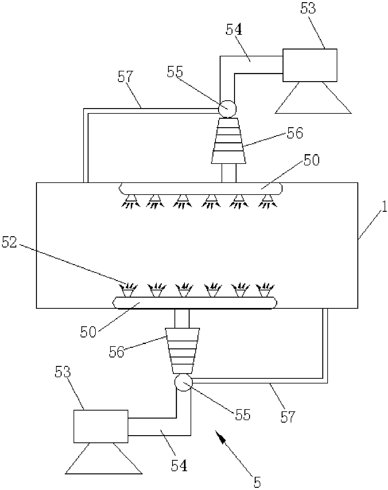
②In the existing electroplating line, pump motors are usually used to supply pressure for the normal circulation of the liquid in the electroplating tank, and then the liquid is sprayed out through the nozzle; as we all know, when the thickness of the PCB board is inconsistent, the required spray flow will inevitably be different. Changes, such as: when electroplating ultra-thin copper-clad laminates, the required spray flow rate is reduced by more than 50% compared with conventional plate thickness, which means that when electroplating ultra-thin copper-clad laminates, the pump motor sprays If the liquid pressure is reduced by 50%, it will inevitably lead to pressure backflow and damage the pump, greatly shortening the service life of the pump motor

Method used


Image

  • pcb plating line
  • pcb plating line

Examples


Embodiment 1

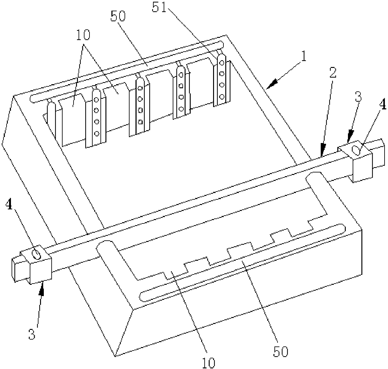
[0029] Please refer to the attached figure 1 As shown, it is a schematic diagram of the partial structure of the PCB electroplating line of the present invention. The PCB electroplating line includes an electroplating tank 1 for holding an electroplating solution, several flying targets 2 and several copper plates (not shown in the figure), and the electroplating tank 1 has a tank bottom and a wall around the bottom of the tank Two pairs of side walls, and a pair of side walls arranged opposite to each other on the electroplating tank 1 are symmetrically provided with a number of fixed bases arranged at intervals, and the number of flying targets 2 are all electrically connected to the negative pole of the power supply, and Each of the flying targets 2 is erected respectively between the two symmetrical fixed bases, and each of the flying targets 2 is also hung with clamps for clamping the PCB board to be plated; the several The copper plates are all electrically connected to...


PUM


Abstract

The invention discloses a PCB (Printed Circuit Board) plating line, which comprises a plating bath, a plurality of tow gliders and a plurality of copper plates. The plating bath is provided with a bath base and two pairs of side vertical walls surrounding the periphery of the bath base; a plurality of fixing bases are symmetrically arranged on one pair of side vertical walls arranged oppositely on the plating bath; the tow gliders are electrically connected to a power supply cathode; each tow glider is erected between each two symmetric fixing bases; a fixture is also arranged on each tow glider in a suspending way; the copper plates are electrically connected to a power supply anode, are symmetrically arranged on the plating bath, and are oppositely arranged on inner surfaces of the other pair of side vertical walls; a vibrating motor is connected onto each tow glider; and a vibrating sensor is also arranged on each vibrating motor, and is electrically connected to a control system. Therefore, the vibrating information of the vibrating motors can be collected and saved in real time, and not only are the monitoring accuracy and the efficiency improved, but also the operating personnel can conveniently adjust and check the vibrating conditions of the vibrating motors in real time.

Description

technical field [0001] The invention relates to the technical field of PCB circuit boards, and specifically provides a PCB electroplating line. Background technique [0002] The miniaturization of electronic products has brought a series of challenges to the component manufacturing and printed circuit board processing industry. The smaller the product, the greater the degree of component integration. For component manufacturers, the solution is to increase the unit The number of pins in terms of area, IC component packaging has changed from QFP, TCP to BGA, CSP, and is developing towards higher-order FC at the same time. Correspondingly, the HDI line width / spacing has also changed from 4mil / 4mil (100μm / 100μm) to 3mil / 3mil (75μm / 75μm), and even the current 60μm / 60μm; its internal structure and processing technology are also constantly changing. Changes to meet its thinner, denser, smaller requirements. [0003] HDI develops to realize the high-density arrangement of BallArr...

Claims


Application Information

Patent Timeline
Patent Type & Authority Patents(China)
IPC IPC(8): C25D7/12C25D17/00
CPCC25D7/12C25D17/00
Inventor 李泽清
Owner 竞陆电子(昆山)有限公司
Learn More