Image pixel sensor pixel structure of hole transmission

An image sensor and pixel structure technology, applied in the field of image sensors, can solve the problems of high output noise of NMOS tubes, large parasitic capacitance in the floating active area, and low sensitivity, so as to enhance the ability of anti-radiation, improve image quality, and improve the user experience. The effect of light efficiency

Pending Publication Date: 2016-11-09
BEIJING SUPERPIX MICRO TECHNOLOGY CO LTD
View PDF10 Cites 4 Cited by
  • Summary
  • Abstract
  • Description
  • Claims
  • Application Information

AI Technical Summary

Problems solved by technology

[0005] Since the output noise of the NMOS tube itself is relatively high, and it is also connected to the entire P substrate, the noise of the peripheral circuit is easily conducted to the transistor through the substrate, which aggravates the output noise and affects the output image effect; the dark photodiode in the prior art The current is large, and white spots will be generated when the image sensor outputs the image, which will affect the output image effect
[0006] Due to the small photosensitive area and low sensitivity of the small-area pixel sensor, the information transmitted in dark light is not clear enough
Especially when the first layer of metal, the second layer of metal and the third layer of metal are used as device interconnection lines, the dielectric height on the surface of the photodiode Si (silicon) is relatively high, and the metal line blocks part of the light from entering the photodiode; Moreover, the metal line connecting the floating active area to the gate of the source follower transistor is close to the power supply metal line, and the parasitic capacitance of the floating active area is large, resulting in a small amplitude (conversion gain) for converting signal electrons into signal voltage

Method used


Image

  • Image pixel sensor pixel structure of hole transmission
  • Image pixel sensor pixel structure of hole transmission
  • Image pixel sensor pixel structure of hole transmission

Examples


Embodiment Construction

[0029] The technical solutions in the embodiments of the present invention will be clearly and completely described below in conjunction with the accompanying drawings in the embodiments of the present invention. Obviously, the described embodiments are only some of the embodiments of the present invention, not all of them. Based on the embodiments of the present invention, all other embodiments obtained by persons of ordinary skill in the art without making creative efforts belong to the protection scope of the present invention.

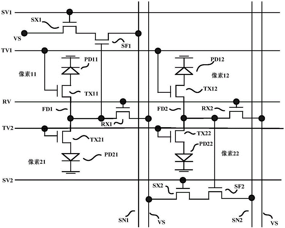
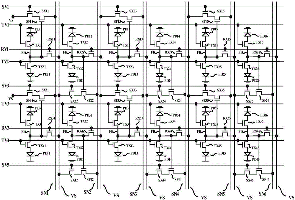
[0030] An embodiment of the present invention provides an image sensor pixel structure for transporting holes, including: multiple groups of pixel units arranged in a two-dimensional pixel array in the vertical and horizontal directions; wherein, each group of pixel units is arranged as four pixels 2×2 pixel array;

[0031] In each group of pixel units, the two pixels in the front row and the two pixels in the rear row respectively share the select...


PUM


Abstract

The invention discloses an image pixel sensor pixel structure of hole transmission. Each group of pixel unit transistors of the structure is a PMOS transistor. Since a PMOS transistor has smaller output noise, the output noise can be reduced, and since PMOS transistors are placed inside an N well, the noise of peripheral devices can be isolated. Each group of pixel unit transistors can effectively reduce dark current and increase anti-irradiation capability. In the hole transmission image sensor 2D pixel array, two layers of metal lines are used to connect metal connecting lines, and only the zero layer of metal lines and the first layer of metal lines are used for serving as control lines of a device to acquire image information, and the second layer or higher layer of metal lines are not used as control lines of the device, so that the height of the medium on the surface of the photodiode Si and more light can radiate to the photodiode, and light usage efficiency and transition gain of small-area pixel sensor can be increased and sensitivity can be increased; in addition, the structure can effectively increase image quality of the small-area pixel sensor.

Description

technical field [0001] The present invention relates to the technical field of image sensors, in particular to an image sensor pixel structure for transporting holes. Background technique [0002] Image sensors have been widely used in digital cameras, mobile phones, medical devices, automobiles and other applications. In particular, the rapid development of technologies for manufacturing CMOS (Complementary Metal Oxide Semiconductor) image sensors and CCD (Charge Coupled Device) image sensors has made people have higher requirements for the output image quality of image sensors. [0003] The CMOS image sensor columns in the prior art share the arrangement of the 2×2 pixel unit structure. Taking 4T2S (four transistors and two pixels sharing) as an example, due to the dependence on the structural characteristics of the pixel itself, the transistors in the prior art are all NMOS The output noise of the NMOS tube itself is higher than that of the PMOS tube, and the dark curren...

Claims


Application Information

Patent Timeline
IPC IPC(8): H01L27/146
CPCH01L27/14643
Inventor 王壮旷章曲刘志碧李文杰李轩陈多金
Owner BEIJING SUPERPIX MICRO TECHNOLOGY CO LTD
Why Eureka
Try Eureka