Active Clamp Flyback Circuit and Its Control Method
A technology of flyback circuit and clamping circuit, which is applied in the direction of control/regulation system, electrical components, and adjustment of electrical variables, etc., can solve the problems of difficult optimization of light-load efficiency, large no-load power consumption, and low light-load efficiency, and achieve Flexible control scheme, reduced no-load power consumption, and reduced voltage
- Summary
- Abstract
- Description
- Claims
- Application Information
AI Technical Summary
Problems solved by technology
Method used
Image
Examples
Embodiment 1
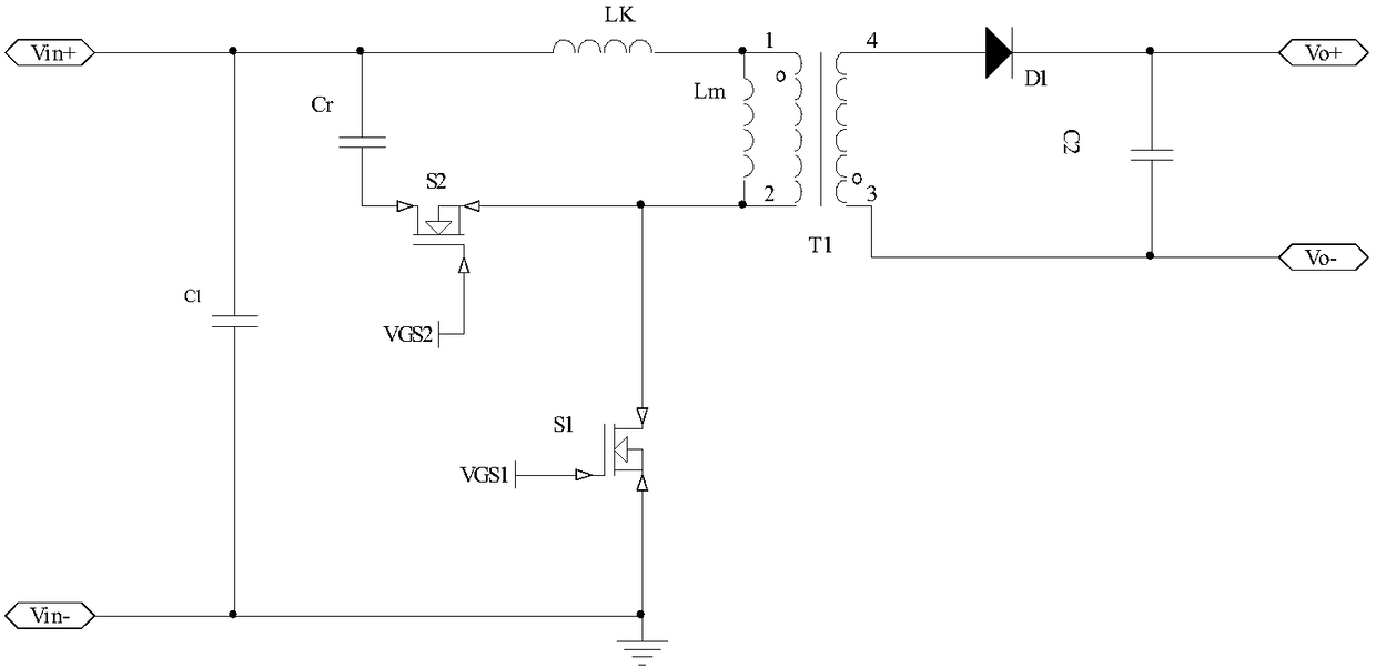
[0029] like Figure 4 As shown, it is the circuit schematic diagram of the active clamping flyback circuit of the present invention, the circuit adds a clamping diode D2 on the basis of the traditional active clamping flyback circuit, and the cathode of the clamping diode is connected to the terminal of S2 At the drain terminal, the anode of the clamp diode is connected to the bus terminal, and the diode is connected in parallel with the clamp capacitor.
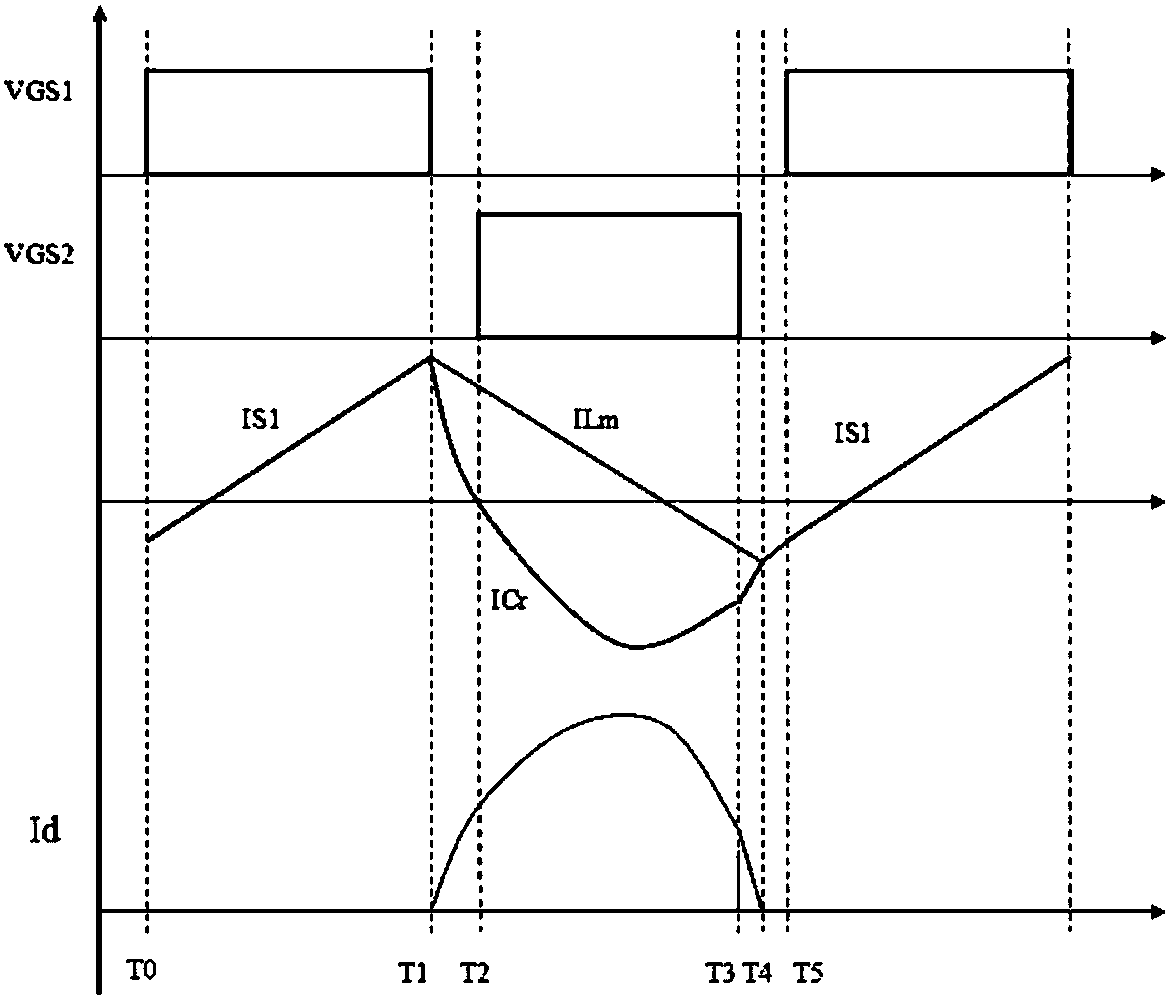
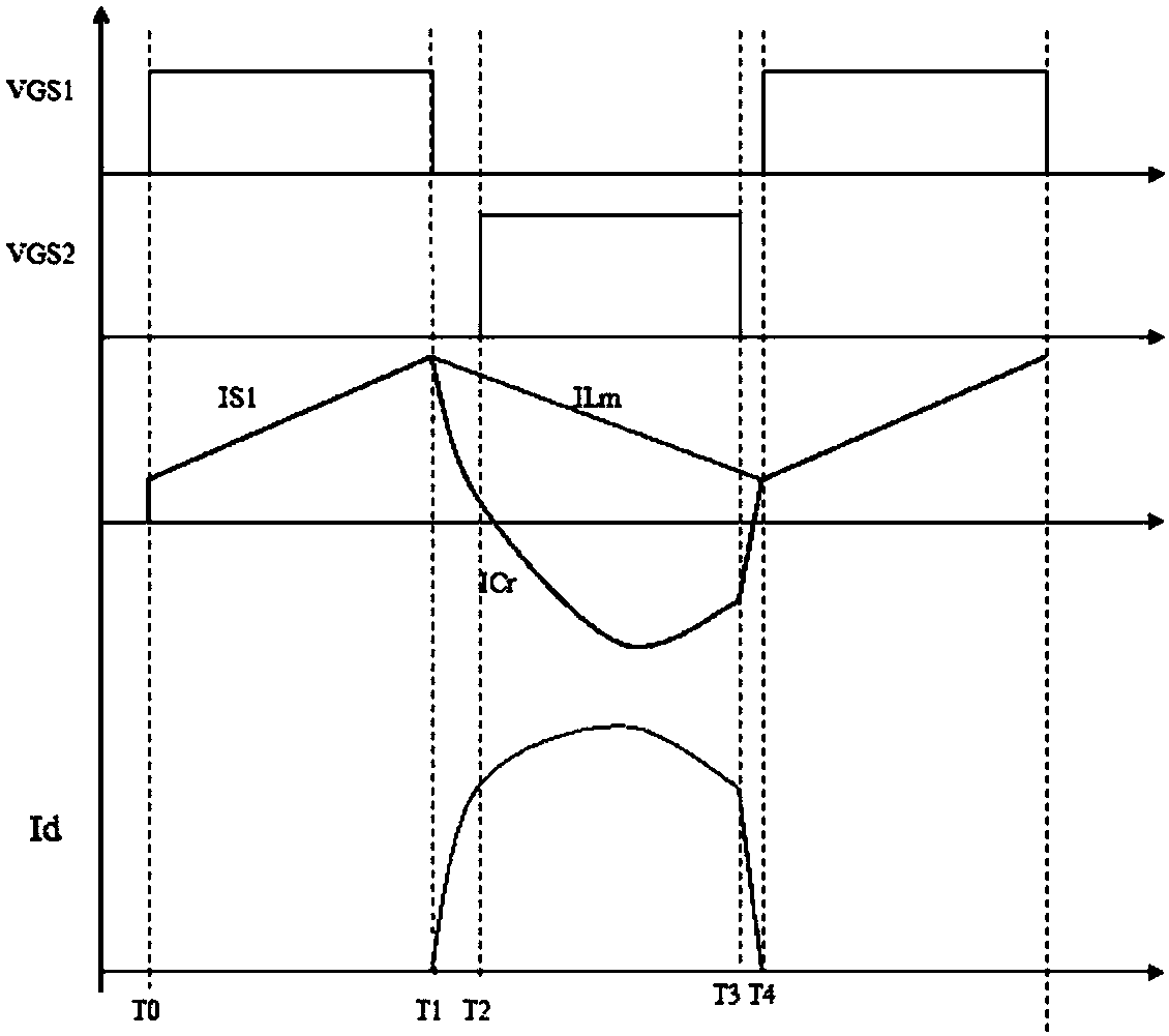
[0030] like Figure 5 As shown, it is the working waveform diagram of the active clamp flyback circuit of the present invention under full load. The specific working principle of the circuit is that at T0 time, the switch tube S1 is turned on, the input voltage is negatively demagnetized to the exciting inductor, and the exciting current After zero-crossing, it is positively excited, and the current flows from the voltage input terminal to the transformer and then flows through the switch tube S1. No current flows through the...
Embodiment 2
[0036] like Figure 10 As shown, it is the circuit schematic diagram of the specific embodiment 2 of the active clamping flyback circuit of the present invention. The difference between the active clamping flyback circuit of this embodiment and the first embodiment is that the The clamping diode was replaced with a TVS tube. Compared with the ordinary diode used in the first embodiment, the use of the TVS tube can not only realize the function of the ordinary diode to clamp the excitation inductance voltage, but also suppress the S1 drain voltage in a lower range, and use a smaller In this case, ensure that the drain-source voltage stress of S1 is within a safer range. Its working principle is the same as that in Embodiment 1, so it will not be repeated here.
PUM
 Abstract
Description
Claims
Application Information
 - R&D Engineer
- R&D Manager
- IP Professional
- Industry Leading Data Capabilities
- Powerful AI technology
- Patent DNA Extraction
Browse by: Latest US Patents, China's latest patents, Technical Efficacy Thesaurus, Application Domain, Technology Topic, Popular Technical Reports.
© 2024 PatSnap. All rights reserved.Legal|Privacy policy|Modern Slavery Act Transparency Statement|Sitemap|About US| Contact US: help@patsnap.com


