Manufacturing method for touch screen cover plate
A touch screen and cover technology, which is applied in the input/output process of data processing, instruments, electrical digital data processing, etc., can solve the problems of dull touch screen cover and dull ink gloss.
- Summary
- Abstract
- Description
- Claims
- Application Information
AI Technical Summary
Problems solved by technology
Method used
Image
Examples
preparation example Construction
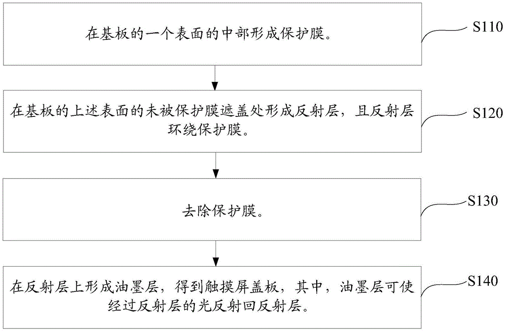
[0032] Such as figure 1 Shown, the preparation method of the touch screen cover plate of an embodiment, comprises the following steps:
[0033] Step S110: forming a protective film in the middle of one surface of the substrate.
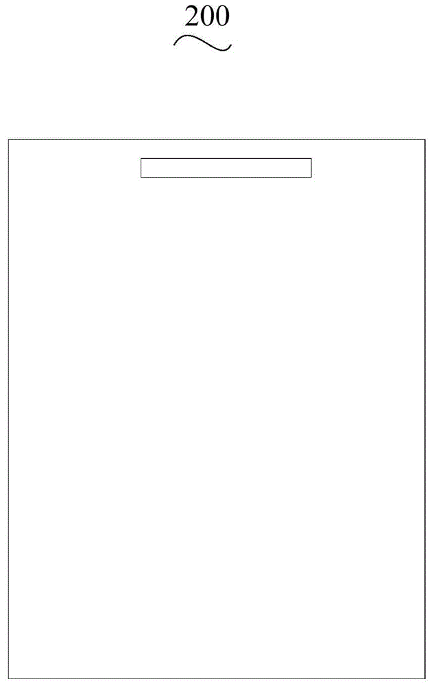
[0034] see figure 2 , figure 2 This is the substrate 200 on which no protective film has been formed.
[0035] Wherein, the substrate is a glass plate, a quartz plate, an alumina plate or a transparent organic plate.
[0036] The thickness of the substrate is 0.01-10 mm; preferably, the thickness of the substrate is 0.1-5 mm; more preferably, the thickness of the substrate is 0.3-2 mm.
[0037] see image 3 and Figure 4 , a protective film 300 is formed in the middle of one surface of the substrate 200 .
[0038] The material of the protective film can be peelable glue or soluble ink.
[0039] The soluble ink can be a water-soluble ink, and it can be understood that the soluble ink is not limited to a water-soluble ink, and any soluble ink ...
Embodiment 1
[0067] The preparation steps of the touch screen cover plate of the present embodiment are as follows:
[0068] (1) transfer peelable blue glue on the middle of one surface of a glass substrate with a thickness of 0.1 mm, and bake at 160° C. for 15 minutes to form a protective film.
[0069] (2) A nickel layer with a thickness of 10 nanometers is formed on the surface of the glass substrate not covered by the protective film by vacuum thermal evaporation, and the nickel layer surrounds the protective film.
[0070] (3) Tear off the protective film, screen-print thermosetting ink on the reflective layer, cure at 150° C. for 20 minutes to form an ink layer with a thickness of 1 mm, and then clean it to obtain a touch screen cover.
[0071] The reflectivity of the touch screen cover plate obtained in this embodiment is tested using a color inversion rate measuring instrument, and the glossiness of the touch screen cover plate obtained in this embodiment is tested using a standard...
Embodiment 2
[0073] The preparation steps of the touch screen cover plate of the present embodiment are as follows:
[0074] (1) Screen-print a water-soluble protective ink on the middle of one surface of a quartz substrate with a thickness of 5 mm, and bake at 150° C. for 15 minutes to form a protective film.
[0075] (2) The magnetron sputtering method is used to form a first silicon dioxide layer with a thickness of 30 nanometers, a first aluminum oxide layer with a thickness of 45 nanometers, a thickness of The second silicon dioxide layer is 45 nanometers, the second aluminum oxide layer is 50 nanometers thick, and the third silicon dioxide layer is 50 nanometers thick, that is, five reflective layers.
[0076] (3) Screen printing thermosetting ink on the third silicon dioxide layer, curing at 130° C. for 30 minutes to form an ink layer with a thickness of 1 nanometer.
[0077] (4) The substrate in step (3) is sprayed with pure water to remove the protective film, and then cleaned to...
PUM
| Property | Measurement | Unit |
|---|---|---|
| Thickness | aaaaa | aaaaa |
| Thickness | aaaaa | aaaaa |
| Thickness | aaaaa | aaaaa |
Abstract
Description
Claims
Application Information
 - R&D
- Intellectual Property
- Life Sciences
- Materials
- Tech Scout
- Unparalleled Data Quality
- Higher Quality Content
- 60% Fewer Hallucinations
Browse by: Latest US Patents, China's latest patents, Technical Efficacy Thesaurus, Application Domain, Technology Topic, Popular Technical Reports.
© 2025 PatSnap. All rights reserved.Legal|Privacy policy|Modern Slavery Act Transparency Statement|Sitemap|About US| Contact US: help@patsnap.com


