Capacitive flexible pressure sensor based on composite material dielectric layer and preparation method of capacitive flexible pressure sensor
A pressure sensor and composite material technology, applied in the field of sensors, can solve the problems such as the sensitivity and stability of the sensor need to be further improved, and achieve the effects of being beneficial to application promotion, improving sensitivity, and improving rate of change
- Summary
- Abstract
- Description
- Claims
- Application Information
AI Technical Summary
Problems solved by technology
Method used
Image
Examples
Embodiment 1
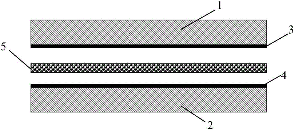
[0064] (1) Preparation of flexible substrate
[0065] Commercially available polydimethylsiloxane (PDMS) monomer and curing agent (Dow Corning, SYLGARD 184, the United States) were thoroughly mixed according to a mass ratio of 10:1, and OSP-100 Meyer rods (OSP-100 , Shijiazhuang Aospa Machinery Technology Co., Ltd.) on the surface of commercially available inkjet printing paper (Canon, LU-101 professional suede photo paper, Japan), and then put it in a vacuum oven for 5 minutes at room temperature to remove the coating. Bubbles in the layer, cured at 70°C for 2 hours, and peeled off from the surface of the photo paper to obtain a flexible substrate with a thickness of 100 μm.
[0066] (2) Preparation of conductive layer and electrodes
[0067] Using screen printing (screen printing machine: OS-500FB, China Outlet Printing Machinery Industry Co., Ltd.), print nano-silver conductive ink (AP02, Beijing Beiyin Zhongyuan Technology Co., Ltd.) on the surface of the flexible substra...
Embodiment 2
[0077] (1) Preparation of flexible substrate
[0078] The commercially available dimethylsiloxane (PDMS) monomer and curing agent (Dow Corning, SYLGARD 184, the United States) were thoroughly mixed at a mass ratio of 10:1, and OSP-1.5 Meyer rods (OSP-1.5, Shijiazhuang Austrian Machinery Technology Co., Ltd.) on the surface of commercially available inkjet printing photo paper (Canon, LU-101 professional suede photo paper, Japan), and then put it in a vacuum oven for 5 minutes at room temperature to remove the coating medium air bubbles, cured at 70°C for 2 hours, and peeled off from the surface of the photo paper to obtain a flexible substrate with a thickness of 1 μm.
[0079] (2) Preparation of conductive layer and electrodes
[0080] On the surface of the flexible substrate, the carbon nanotube conductive layer (TNWPM, Chengdu Organic Chemistry Co., Ltd., Chinese Academy of Sciences) was prepared by coating the OSP-1.5 Meyer rod (OSP-1.5, Shijiazhuang OSP Machinery Technol...
Embodiment 3
[0089] Other is exactly the same as embodiment 1, and difference is:
[0090] (1) Replace "polydimethylsiloxane (PDMS) / silver nanoparticle composite material" with "polystyrene (PS), epoxy resin, polyvinylidene fluoride (PVDF), polyester (PET), Polycarbonate (PC), polyphenylene sulfide (PPS), polypropylene (PP), polyimide (PI), polyethylene 2,6-naphthalene (PEN), polyurethane, polyurethane acrylate, Organic glass, silicone rubber or UV curable glue / copper, gold, aluminum, lead, zinc or tin nanoparticles (the optimal range of each doping component is 25wt.%~55wt.%) composite material".
[0091] (2) The thickness of the dielectric layer is 1 μm.
PUM
| Property | Measurement | Unit |
|---|---|---|
| Thickness | aaaaa | aaaaa |
| Thickness | aaaaa | aaaaa |
| Surface resistance | aaaaa | aaaaa |
Abstract
Description
Claims
Application Information
 - R&D Engineer
- R&D Manager
- IP Professional
- Industry Leading Data Capabilities
- Powerful AI technology
- Patent DNA Extraction
Browse by: Latest US Patents, China's latest patents, Technical Efficacy Thesaurus, Application Domain, Technology Topic, Popular Technical Reports.
© 2024 PatSnap. All rights reserved.Legal|Privacy policy|Modern Slavery Act Transparency Statement|Sitemap|About US| Contact US: help@patsnap.com


