Compositions for high speed printing of conductive materials for electronic circuitry type applications, and methods relating

A high-speed printing, conductive material technology, applied in applications, household appliances, inks, etc., can solve the problems of limited scalability, low deposition speed, high cost, etc.

Inactive Publication Date: 2016-09-21
EI DU PONT DE NEMOURS & CO
View PDF5 Cites 1 Cited by
  • Summary
  • Abstract
  • Description
  • Claims
  • Application Information

AI Technical Summary

Problems solved by technology

Such techniques are generally capable of high quality conductor deposition, but tend to suffer from low deposition rates, high cost, limited scalability, and / or high processing temperatures

Method used


Image

  • Compositions for high speed printing of conductive materials for electronic circuitry type applications, and methods relating
  • Compositions for high speed printing of conductive materials for electronic circuitry type applications, and methods relating
  • Compositions for high speed printing of conductive materials for electronic circuitry type applications, and methods relating

Examples


preparation example Construction

[0070] The present disclosure also relates to production methods and substrates having conductive metallizations produced by said production methods. The preparation method comprises the following steps:

[0071] (1) Provide the substrate,

[0072] (2) applying the conductive composition of the present invention to a substrate, and

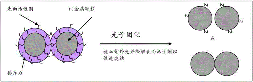
[0073] (3) Subjecting the conductive composition applied in step (2) to photonic sintering to form a conductive metallization.

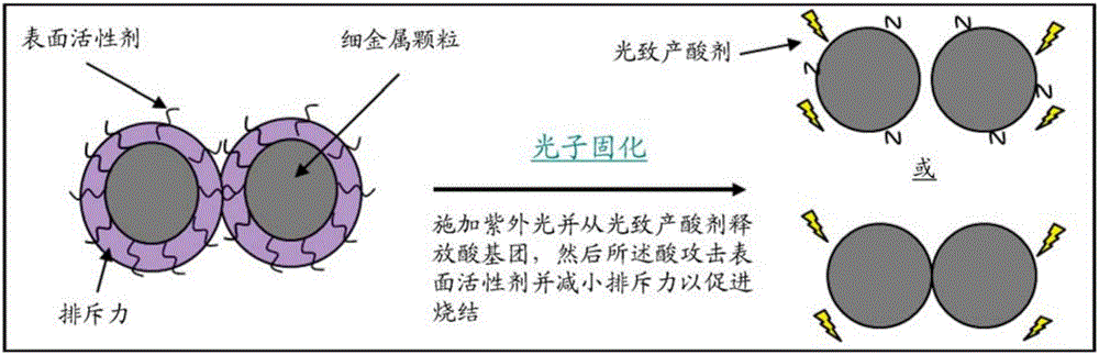
[0074] For embodiments in which the decomposable stabilizer comprises groups acidolyzed by catalytically active methods, photonic sintering can be performed with the aid of photoacid generators as shown in Table 1 below:

[0075]

[0076] Table 1

[0077] The "surfactants" indicated in Table 1 are intended to mean the thermally decomposable stabilizers of the present disclosure, or alternatively may denote co-surfactants in addition to the thermally decomposable stabilizers, wherein in addition to or independently ...


PUM

PropertyMeasurementUnit
particle sizeaaaaaaaaaa
electrical resistanceaaaaaaaaaa

Abstract

The present invention is directed to compositions for high speed printing of conductive materials for electronic circuitry type applications. These compositions are dispersions having a continuous (e.g., solvent) phase and a discontinuous phase. The discontinuous phase includes a plurality of nanoparticles stabilized with a thermally decomposable stabilizer. The thermally decomposable stabilizer is an Phi-b-theta-Y block co-polymer or oligomer where: i. Phi is a polymeric block or series of polymeric blocks that swell and suspend in the continuous phase; ii. b indicates a covalent bond between Phi and theta; iii. theta comprises at least one moiety from the group consisting of tertiary amines, electron rich aromatics, acrylates, methacrylates and combinations thereof; and iv. Y is a dithioester, a xanthate, a dithiocarbamate, a trithiocarbonate or a combination thereof.

Description

technical field [0001] The technical field generally relates to dispersions of conductive nanoparticles that can be destabilized by applying relatively low levels of thermal energy or by using relatively low levels of electromagnetic (e.g., ultraviolet light or microwave) radiation to intentionally cause the nanoparticles to fall out of suspension. exfoliate and form the desired characteristic structure of conductive nanoparticle agglomerates. More specifically, the composition of the present invention is useful for high-speed printing of conductive materials for electronic circuit type applications and the like. Background technique [0002] There is a need to inexpensively fabricate conductive circuit features on circuit boards and other substrates. Typically high vacuum techniques such as sputtering, chemical vapor deposition (CVD) and atomic layer deposition (ALD) are used. Such techniques are generally capable of high quality conductor deposition, but tend to suffer f...

Claims


Application Information

Patent Timeline
Patent Type & Authority Applications(China)
IPC IPC(8): C09D11/52
CPCC09D11/52
Inventor W·B·法纳姆D·辉
Owner EI DU PONT DE NEMOURS & CO
Why Eureka
Try Eureka