Growth method for light-emitting diode epitaxial wafer

A technology of light-emitting diodes and growth methods, which is applied in the field of growth of light-emitting diode epitaxial wafers, can solve the problems of low LED luminous efficiency, and achieve the effects of improving luminous efficiency, crystal quality, and crystal quality

Active Publication Date: 2016-09-21
HC SEMITEK SUZHOU
View PDF8 Cites 7 Cited by
  • Summary
  • Abstract
  • Description
  • Claims
  • Application Information

AI Technical Summary

Problems solved by technology

[0006] In order to solve the problem of low luminous efficiency of LEDs in the prior art, an embodiment of the present invention provides a method for growing a light emitting diode epitaxial wafer

Method used


Image

  • Growth method for light-emitting diode epitaxial wafer

Examples


Embodiment

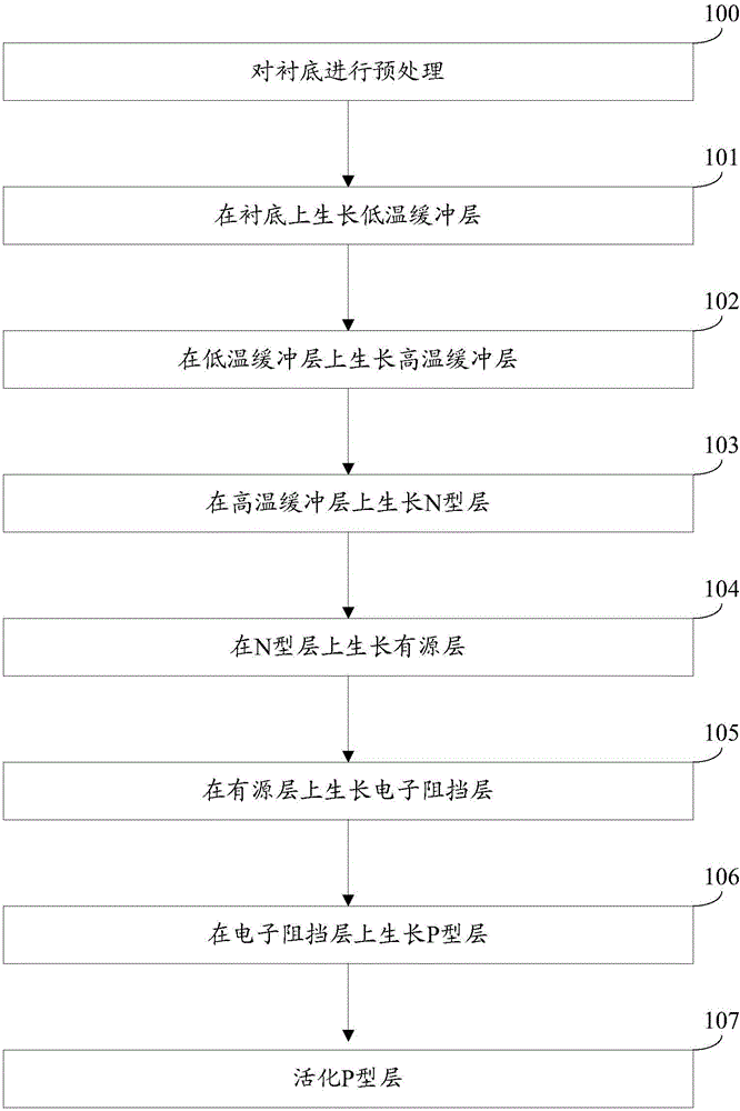
[0025] An embodiment of the present invention provides a method for growing a light-emitting diode epitaxial wafer, see figure 1 , the growth method includes:

[0026] Step 100: Perform pretreatment on the substrate.

[0027] In this embodiment, the substrate is a sapphire substrate.

[0028] Specifically, this step 100 may include:

[0029] Under a hydrogen atmosphere, treat the substrate at a high temperature for 5 min to 6 min. Wherein, the temperature of the reaction chamber is 1000° C. to 1100° C., and the pressure of the reaction chamber is controlled at 200 torr to 500 torr.

[0030] In this embodiment, a Veeco K465i or C4 metal organic chemical vapor deposition (Metal Organic Chemical Vapor Deposition, MOCVD) equipment is used to realize the LED growth method. Using high-purity hydrogen (H 2 ), high-purity nitrogen (N 2 ) or high purity H 2 and high purity N 2 The mixed gas as the carrier gas, high-purity NH 3 As the N source, trimethylgallium (TMGa) and triet...


PUM


Abstract

The invention discloses a growth method for a light-emitting diode epitaxial wafer, and belongs to the technical field of semiconductors. The method comprises the step: sequentially growing a low-temperature buffering layer, a high-temperature buffering layer, an N-type layer, an active layer, an electronic blocking layer and a P-type layer on a substrate. The active layer comprises a first sub-layer and a second sub-layer, and the growth atmospheres of a quantum well layer in the first sub-layer, a quantum barrier layer in the first sub-layer, a quantum well layer in the second sub-layer and a quantum barrier layer in the second sub-layer are sequentially N2 and H2 mixed gas, pure H2, pure N2, and N2 and H2 mixed gas. The quantum well layer in the first sub-layer employs a variable pressure and variable temperature growth mode, and the quantum barrier layer in the first sub-layer employs a high-pressure and high-temperature growth mode. The quantum well layer in the second sub-layer employs a low-pressure and low-temperature growth mode, and the quantum barrier layer in the second sub-layer employs a variable pressure growth mode. The quantum barrier layer in the first sub-layer employs trimethyl gallium as a gallium source. The method improves the light-emitting efficiency.

Description

technical field [0001] The invention relates to the technical field of semiconductors, in particular to a method for growing a light-emitting diode epitaxial wafer. Background technique [0002] Light Emitting Diode (LED for short) is a semiconductor electronic component that can emit light. As a new type of high-efficiency, environmentally friendly and green solid-state lighting source, LEDs are rapidly and widely used in fields such as traffic lights, interior and exterior lights of automobiles, urban landscape lighting, and mobile phone backlights. [0003] The existing LED epitaxial wafer growth method is to sequentially grow a low-temperature buffer layer, a high-temperature buffer layer, an N-type layer, an active layer, and a P-type layer on a substrate, wherein the active layer includes alternately stacked quantum well layers and quantum barriers. layer, quantum well layer and quantum barrier layer growth conditions are kept unchanged. [0004] In the process of re...

Claims


Application Information

Patent Timeline
Patent Type & Authority Applications(China)
IPC IPC(8): H01L33/00
CPCH01L33/007
Inventor 姚振从颖胡加辉
Owner HC SEMITEK SUZHOU
Why Eureka
Try Eureka