N-plane gan-based fin-type high electron mobility transistor and manufacturing method
A technology with high electron mobility and manufacturing method, which is applied in the field of high-speed and low-power integrated circuits, can solve the problems of poor two-dimensional electron gas confinement, high ohmic contact resistance, and weak short-channel effect suppression ability, etc. The effect of small current collapse, improving the switching current ratio, and suppressing the short channel effect
- Summary
- Abstract
- Description
- Claims
- Application Information
AI Technical Summary
Problems solved by technology
Method used
Image


Examples
Embodiment 1
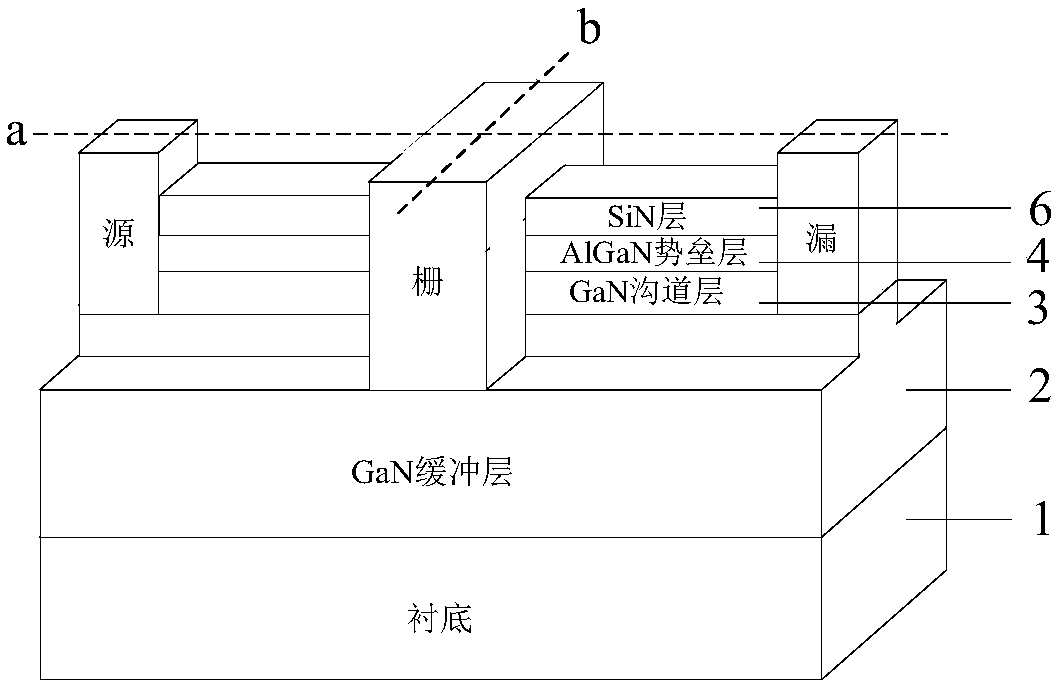
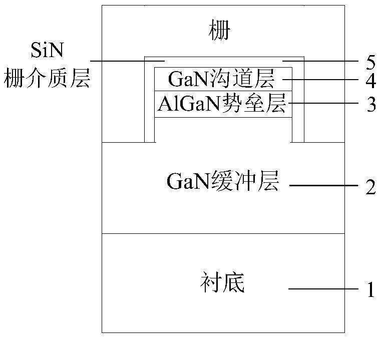
[0031] Embodiment 1: Fabricate an N-plane GaN-based fin-type high electron mobility transistor with a substrate of sapphire, a GaN buffer layer thickness of 1 μm, and a fin-type GaN / AlGaN heterojunction width of 200 nm.
[0032] Step 1: growing a buffer layer.
[0033] exist Figure 4 (a) On the sapphire substrate shown in (a), a layer of N-face GaN buffer layer with a thickness of 1 μm was grown on the sapphire substrate by molecular beam epitaxy MBE. -3 Pa.
[0034] Step 2: growing a barrier layer.
[0035] A layer of AlGaN with a thickness of 20nm was grown on the GaN layer by MBE, and the Al composition gradually changed from 5% to 30% from bottom to top; another layer of AlGaN with a thickness of 10nm and an Al composition of 30% was grown layer, the technological conditions for its growth are: the growth temperature is 680°C, and the pressure is 5×10 -3 Pa.
[0036] Step 3: growing a channel layer.
[0037] On the AlGaN layer, a GaN channel layer with a thickness o...
Embodiment 2
[0050] Embodiment 2: Fabricate an N-plane GaN-based fin-type high electron mobility transistor with SiC substrate, GaN buffer layer thickness of 2 μm, and fin-type GaN / AlGaN heterojunction width of 400 nm.
[0051] Step 1: Growth buffer layer.
[0052] On the SiC substrate, a layer of N-face GaN buffer layer with a thickness of 2 μm is grown by molecular beam epitaxy MBE. The growth process conditions are:
[0053] The growth temperature is 680°C and the pressure is 5×10 -3 Pa.
[0054] Step 2: Growing a barrier layer.
[0055] A layer of AlGaN with a thickness of 20nm was grown on the GaN layer by MBE, and the Al composition gradually changed from 5% to 30% from bottom to top; another layer of AlGaN with a thickness of 8nm and an Al composition of 30% was grown layer, the process conditions for its growth are:
[0056] The growth temperature is 680°C and the pressure is 5×10 -3 Pa.
[0057] Step 3: growing a channel layer.
[0058] On the AlGaN layer, a layer of N-face...
Embodiment 3
[0070] Embodiment 3: Fabricate an N-plane GaN-based fin-type high electron mobility transistor with a SiC substrate, a GaN buffer layer thickness of 2.5 μm, and a fin-type GaN / AlGaN heterojunction width of 500 nm.
[0071] Step A: growing a buffer layer on the substrate.
[0072] Using molecular beam epitaxy MBE equipment at a temperature of 680°C and a pressure of 5×10 -3 Under the process condition of Pa, an N-face GaN buffer layer with a thickness of 2.5 μm is grown on the SiC substrate.
[0073] Step B: growing a barrier layer on the buffer layer.
[0074] Using molecular beam epitaxy MBE equipment at a temperature of 680°C and a pressure of 5×10 -3 Under the process conditions of Pa, a layer of AlGaN with a thickness of 20nm is first grown on the GaN buffer layer, and the Al composition is gradually changed from 5% to 30% from bottom to top, and the thickness of another layer is 5nm, and the Al composition is 30%. AlGaN layer.
[0075] Step C: growing a channel layer ...
PUM
 Abstract
Description
Claims
Application Information
 - Generate Ideas
- Intellectual Property
- Life Sciences
- Materials
- Tech Scout
- Unparalleled Data Quality
- Higher Quality Content
- 60% Fewer Hallucinations
Browse by: Latest US Patents, China's latest patents, Technical Efficacy Thesaurus, Application Domain, Technology Topic, Popular Technical Reports.
© 2025 PatSnap. All rights reserved.Legal|Privacy policy|Modern Slavery Act Transparency Statement|Sitemap|About US| Contact US: help@patsnap.com