Monocrystalline silicon double-sided solar cell and preparation method thereof
A technology of double-sided solar cells and monocrystalline silicon, which is applied in the field of solar cells to achieve the effects of improving quantum conversion efficiency, simple process, and reducing surface area
- Summary
- Abstract
- Description
- Claims
- Application Information
AI Technical Summary
Problems solved by technology
Method used
Image
Examples
Embodiment 1
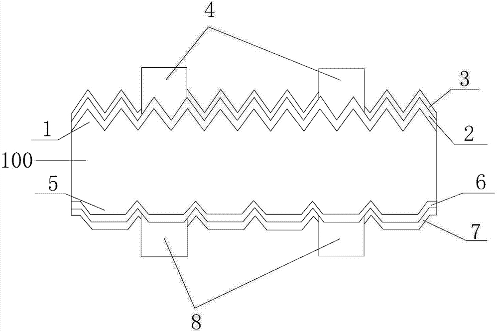
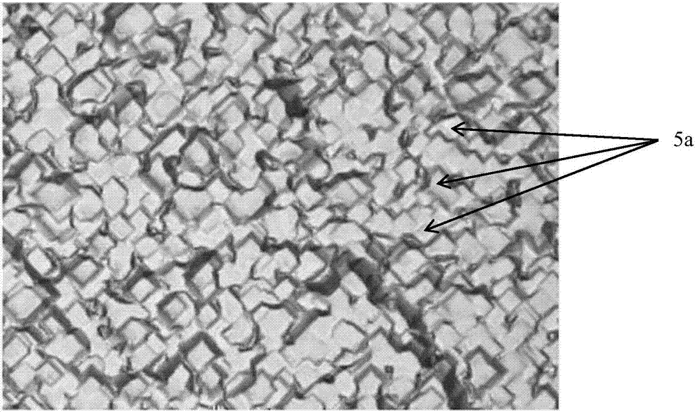
[0029] This embodiment is the case where the present invention is applied to P-type single crystal silicon. Such as figure 1 As shown, on the front side of the P-type single crystal silicon substrate 100, a front textured topographic structure 1 is sequentially formed, in this embodiment, it is a front pyramid-shaped textured surface, a front phosphorus-doped emitter junction 2, and a front passivation anti-reflection medium. layer 3 and the front electrode 4, on the back of the P-type single crystal silicon substrate, the back texturing topography structure 5, the boron-doped back surface field 6 formed by boron doping on the back, the back passivation anti-reflection dielectric layer 7 and back electrode 8, where, as figure 2 As shown, the back surface texture structure 5 is a platform-shaped suede surface, and each platform structure 5a is scattered, or partially connected, or partially overlapped, or distributed on the silicon substrate in a partially dispersed, partiall...
Embodiment 2
[0032] The difference between this embodiment and Embodiment 1 lies in that in the textured topography structure 5 on the back, each platform structure 5 a is distributed on the silicon substrate in a partially dispersed and partially connected manner. The side length of the plane on the platform structure 5 a is 10 μm, and the height of the platform structure 5 a is 8 μm. The front passivation anti-reflection medium layer 3 is a single-layer film made of silicon oxynitride with a film thickness of 70 to 80 nm; the back passivation anti-reflection medium layer 7 is a double-layer film made of titanium oxide and silicon oxide, wherein, The titanium oxide film has a thickness of 20 to 30 nm and the silicon oxide film has a thickness of 50 to 70 nm. Both the front electrode 4 and the back electrode 8 are copper electrodes.
Embodiment 3
[0034] This embodiment is a case where the present invention is applied to N-type single crystal silicon. Such as figure 1 As shown, on the front side of the N-type single crystal silicon substrate 100, a front pyramid-shaped textured surface 1, a front boron-doped emitter junction 2, a front passivation anti-reflection dielectric layer 3, and a front electrode 4 are sequentially formed. The back surface of the silicon substrate is sequentially formed with a back textured topographic structure 5, a phosphorus-doped back surface field 6 formed by phosphor doping on the back, a back passivation anti-reflection dielectric layer 7, and a back electrode 8, wherein the back textured topographic structure 5 is a platform-shaped suede surface, and each platform structure 5a is dispersedly distributed on the silicon substrate. Such as figure 1 As shown, the platform structure 5a has a lower plane connected to the silicon substrate 100 and an upper plane opposite to the lower plane. T...
PUM
 Abstract
Description
Claims
Application Information
 - R&D
- Intellectual Property
- Life Sciences
- Materials
- Tech Scout
- Unparalleled Data Quality
- Higher Quality Content
- 60% Fewer Hallucinations
Browse by: Latest US Patents, China's latest patents, Technical Efficacy Thesaurus, Application Domain, Technology Topic, Popular Technical Reports.
© 2025 PatSnap. All rights reserved.Legal|Privacy policy|Modern Slavery Act Transparency Statement|Sitemap|About US| Contact US: help@patsnap.com


